Faculty Research Spotlight: Luke Theogarajan
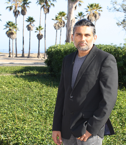
Q & A with Luke Theogarajan, ECE Associate Professor
Biomimetic Circuits & Nanosystems Group
Interviewed for Convergence: The Magazine of Engineering and the Sciences at UCSB (Summer 2014)
Before joining the faculty at UC Santa Barbara’s College of Engineering, Luke Theogarajan lent his circuit designing expertise to Intel for five years as part of the Pentium 4 design team. An electrical engineer by training, Theogarajan has a Ph.D. in electrical engineering and computer science from Massachusetts Institute of Technology.
However, his talents aren’t limited to the world of computers. Theogarajan’s research interests have applications in fields as diverse as biomedicine and energy efficiency, thanks to collaborations with various researchers on campus. His work has earned him four patents and prestigious recognition, including the 2010 NIH New Innovator Award and a 2011 NSF Career Award.
Theogarajan, who heads the Biomimetic and Nanosystems Group, is a founding faculty member for UCSB’s Center for Bioengineering, and designed the undergraduate curriculum for a new Bioengineering emphasis for College of Creative Studies biology majors. He has also received a Northrup Grumman Excellence in Teaching Award in 2011 and was named outstanding faculty member in the electrical engineering department for four years straight.
Convergence interviewed Theogarajan about his work and the many applications that have come from it.
C: What are the main areas of research in which you’re concentrating right now?
LT: I can broadly classify my work in two areas. One is in biomedical engineering, and the other one is in high-speed communications, which actually grew out of some research I was doing in biomedical engineering, but fundamentally, neural interfaces is the one thing that I’ve dedicated my life to.
C: You started your work with neural interfaces before you came to UCSB; tell us what kind of work you’ve done.
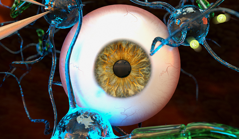
As a graduate student at MIT, the main work I did there was to develop an electrical implant that goes inside the eye and stimulates the retina, eventually sending information to the brain.
In the middle of my Ph.D., I changed direction. I realized that if a visual prosthesis of any significance is going to be developed at some point there has to be a different interface to the nervous system. It cannot be electrical, because the power required for the distance the current needed to travel would generate too much heat eventually leading to cell death. Current implants have limited number of electrodes to around 64-100, which pales in comparison to the 140 million photoreceptors in the eye. So if you are using a limited number of electrodes then it is imperative that you know the precise relationship between electrical stimulation and the neural code sent to the brain, which has not been deciphered yet.
What we’ve been trying to concentrate on is a chemical interface, because if you deliver a sufficient amount of potassium ions local to the neuron, it will actually make the neuron fire, because it upsets the chemical balance. So the question then was: How do you actually make a device that can uptake potassium from the body and release it on command? You have to make a system that almost mimics a real living cell.
What is fundamentally needed for a chemical prosthesis is a scaffold by which you can mimic neurons. You want to make artificial channels and membranes. We developed a system where we take a very thin inorganic membrane about 30 nanometers thick and drilled very tiny holes using a focused electron beam, creating a structural ion channel scaffold. Once we had the structural motif, we needed to enable the functionality of recognition. What we’re doing now is to attach a recognition molecule in the interior of the pore so it selectively moves things across.
C: Your research into biomimetic materials has other applications as well.
Originally, when I was doing my Ph.D, I had to figure out a way to make a synthetic molecule that behaved like a lipid, so I made a polymer system based on previous research that was done by others, and I modified it to the purposes that I needed. That ended up having interesting properties that are useful for drug delivery. We just published a paper about making very modular blocks using “click” chemistry, which is a popular way of coupling polymers together.
We are also studying how these polymers interact with the innate immune system. Anytime a drug delivery system is introduced into your body, the first thing your body’s going to do is recognize whatever you put in and take it out of circulation. You have to impart a stealth property to anything you do in drug delivery so it avoids detection. Using a complement activation assay, we proved that yes, if you use these materials, you’re going to get stealth behavior, provided you don’t use certain types of copper coupling chemistry. Craig Hawker [UCSB professor of materials and chemistry] was a real source of inspiration. I was completely brought up in a different field; I’m a formally trained circuit designer.
The ion channel work can also be applied to the field of single molecule detection, especially DNA sequencing. We have married the world of electronics (i.e. CMOS) with the nanopore (a tiny hole in an insulating membrane) and by monitoring the ion current flowing through this membrane one can perform single molecule detection. We try to thread the DNA through these holes and look at the amount of current that they can block. You can also tell other characteristics like protein folding and misfolded Alzheimer’s proteins using the same technique.
One key issue in these detection platforms is the baseline background current can dwarf the change in ionic current due to the biomolecule. Because we have a strong expertise in electronics, we built a new electronic platform that can distinguish very small changes on very large backgrounds.
Finally, if a useful system is to be designed, a way of coupling the sensor, the electronics and the microfluidics are necessary. Each of these domains operate in a different length scale: the nanoscale, microscale and macroscale, respectively. However, if you make an electronic chip larger just for interfacing the cost goes up exponentially and the yield drops dramatically. So to circumvent this we take a very small chip and make it look very large at a reduced cost, enabling the coupling to the microfluidics. The same technology can be used for integrating electronics and photonics, which is how I started working with John Bowers, who is known around the world for his expertise in optics and photonics.
C: Your work in biotechnology actually benefitted John Bowers’ work in energy efficiency? Tell us more about that.
Yes, I realized that if you use a photonic wafer rather than a dummy silicon wafer like we did with our biorelated work, then very intimate connections can be made between the photonics and electronics. This enables very short electrical interconnects and thus lowers the power of the system, which is essential for energy efficient communications. We also have a grant with DARPA on electronic/photonic integration to implement advanced communication systems using electronics coupled with photonics. John has been a great mentor to me, he’s a fantastic guy.
C: You mentioned that you were essentially dedicated to creating neural interfaces. Aside from the visual prosthesis work and biomimetic cell membrane, what else are you working on?
We’re also working neural recording arrays for brain implants, to help paraplegics or people with neurological damage. For example if the connection between the brain and motor function is damaged one can record from the brain and then stimulate the muscle or control a robotic arm, partially replacing lost function.
One of the big problems in this area is that these implants are made of silicon or stainless steel. However, the modulus of the electrode is so stiff, because it has to withstand the pressure of implantation, that micro shearing happens on the brain, so it develops inflammation. One of the things we’re trying to do is make some arrays that do not have this shearing, using materials that are soft and flexible. We have developed a flexible polymer array with soft electrodes, and are starting a collaboration with the Department of Bioengineering at UC San Diego to test them.
The last question we ask is: how do you mimic brain function? How do you make circuits behave like a brain? How do you make them learn? We have a multiuniversity collaboration (MURI), funded by the Air Force headed by Tim Cheng and Dmitri Strukov, who is an expert in memristor technology (memory resistor – a resistor that remembers). We want to use the memristor as a learning synapse and use that synapse to create artificial circuits that behave like neural system and does tasks of recognition.
Learn more about Theogarajan's research at the Biomimetic Circuits & Nanonsystems Group