IBM Power Grid
Benchmarks
All the power grid benchmarks presented in
this website are drawn from real designs, and vary over a reasonable
range of size and difficulty. They are generated in Spice format. We
hope these benchmarks will motivate new research in this area, and
result in breakthroughs in this challenging problem.
Contact
Prof. Peng Li,
Electrical and Computer Engineering, UC Santa Barbara, Email: lip at ucsb
dot edu.
Acknowledgement
Dr.
Zhuo Li:
Cadence Design Systems (formerly with IBM Austin Research
Lab)
Dr.
Sani R. Nassif: Radyalis LLC (formerly
with IBM Austin Research Lab)
Dr.
Albert Zhiyu Zeng: Cadence Design
Systems (formerly with Texas A&M University)
IBM
Power Grid Benchmarks
IBM Power Grid Benchmarks for DC Analysis
|
Name |
#i |
#n |
#r |
#s |
#v |
#l |
Benchmark Files |
||
|
Voltage Map |
SPICE Netlist |
Solution |
|||||||
|
ibmpg1 |
10774 |
30638 |
30027 |
14208 |
14308 |
2 |
|||
|
ibmpg2 |
37926 |
127238 |
208325 |
1298 |
330 |
5 |
|||
|
ibmpg3 |
201054 |
851584 |
1401572 |
461 |
955 |
5 |
|||
|
ibmpg4 |
276976 |
953583 |
1560645 |
11682 |
962 |
6 |
|||
|
ibmpg5 |
540800 |
1079310 |
1076848 |
606587 |
539087 |
3 |
|||
|
ibmpg6 |
761484 |
1670494 |
1649002 |
836107 |
836239 |
3 |
|||
|
ibmpg7 |
357930 |
1461036 |
2352355 |
461 |
955 |
NA |
NA |
NA |
|
|
ibmpg8 |
357930 |
1461039 |
1422830 |
929722 |
930216 |
NA |
NA |
NA |
|
IBM Power Grid Benchmarks for Transient Analysis
|
Name |
#i |
#n |
#r |
#s |
#v |
#l |
Benchmark Files |
||
|
Voltage Map |
Spice Netlist |
Solution |
|||||||
|
ibmpg1t |
NA |
NA |
NA |
NA |
NA |
NA |
NA |
||
|
ibmpg2t |
NA |
NA |
NA |
NA |
NA |
NA |
NA |
||
|
ibmpg3t |
NA |
NA |
NA |
NA |
NA |
NA |
NA |
||
|
ibmpg4t |
NA |
NA |
NA |
NA |
NA |
NA |
NA |
||
|
ibmpg5t |
NA |
NA |
NA |
NA |
NA |
NA |
NA |
||
|
ibmpg6t |
NA |
NA |
NA |
NA |
NA |
NA |
NA |
||
・
i for current source
・
n
for nodes (total number, does not take shorts into account)
・
r
for resistors (include shorts)
・
s
for shorts (zero value resistors and voltage sources)
・
v
for voltage sources (include shorts)
・
l
for metal layers
・
Other
available
files: README.txt, MD5SUMS.txt, SUMMARY.txt
・
All
the
IBM DC power grid benchmarks are described in detail in: S. R. Nassif, Power Grid Analysis Benchmarks, ASPDAC
2008
SPICE Netlist Gneration
The link between the SPICE
netlist naming and numbering scheme for the circuit and the original
geometry of the power grid is described below.
・
Node name:
n<net-index>_<x-location>_<y-location>
・
Data
associated with each layer starts from:
* layer: <name>,<net>_net:
<net-index>
Each
layer/net combination is associated with a unique net-index.
・ Vias starts from:
* vias from:
<net-index> to <net-index>
Vias
are implemented as resistors or as zero voltage sources.
・
Current
source:
iB<block-number>
<node>
0 <value> and iB<block-number>
0
<node> <value>
Each
current source is split into two components: from VDD to
ideal ground and from ideal ground to VSS. Current
sources in transient benchmarks are pulse current souces.
・ Each circuit file has a global VDD voltage source and each package connection is recognized as a resistor connected to the global source.
Example
of SPICE Netlist Generation
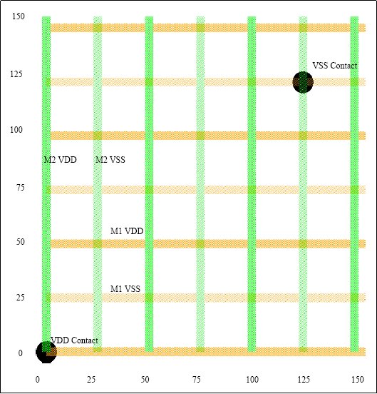
Fig. 1: A small power grid
rr0 n3_0_0 _X_n3_0_0 0.5
v1 _X_n3_0_0 0 1
rr2 n2_125_125 _X_n2_125_125 0.5
v3 _X_n2_125_125 0 0
* layer: M1,VDD net: 1
R4 n1_0_0 n1_50_0 1.25
R5 n1_50_0 n1_100_0 1.25
R6 n1_100_0 n1_150_0 1.25
R7 n1_0_50 n1_50_50 1.25
R8 n1_50_50 n1_100_50 1.25
R9 n1_100_50 n1_150_50 1.25
R10 n1_0_100 n1_50_100 1.25
R11 n1_50_100 n1_100_100 1.25
R12 n1_100_100 n1_150_100 1.25
R13 n1_0_150 n1_50_150 1.25
R14 n1_50_150 n1_100_150 1.25
R15 n1_100_150 n1_150_150 1.25
* vias from: 1 to 3
V16 n1_0_0 n3_0_0 0.0
V17 n1_0_50 n3_0_50 0.0
V18 n1_0_100 n3_0_100 0.0
V19 n1_0_150 n3_0_150 0.0
V20 n1_50_0 n3_50_0 0.0
V21 n1_50_50 n3_50_50 0.0
V22 n1_50_100 n3_50_100 0.0
V23 n1_50_150 n3_50_150 0.0
V24 n1_100_0 n3_100_0 0.0
V25 n1_100_50 n3_100_50 0.0
V26 n1_100_100 n3_100_100 0.0
V27 n1_100_150 n3_100_150 0.0
V28 n1_150_0 n3_150_0 0.0
V29 n1_150_50 n3_150_50 0.0
V30 n1_150_100 n3_150_100 0.0
V31 n1_150_150 n3_150_150 0.0
* layer: M2,VDD net: 3
R32 n3_0_0 n3_0_50 1.25
R33 n3_0_50 n3_0_100 1.25
R34 n3_0_100 n3_0_150 1.25
R35 n3_50_0 n3_50_50 1.25
R36 n3_50_50 n3_50_100 1.25
R37 n3_50_100 n3_50_150 1.25
R38 n3_100_0 n3_100_50 1.25
R39 n3_100_50 n3_100_100 1.25
R40 n3_100_100 n3_100_150 1.25
R41 n3_150_0 n3_150_50 1.25
R42 n3_150_50 n3_150_100 1.25
R43 n3_150_100 n3_150_150 1.25
* layer: M1,GND net: 0
R44 n0_25_25 n0_75_25 1.25
R45 n0_75_25 n0_125_25 1.25
R46 n0_25_75 n0_75_75 1.25
R47 n0_75_75 n0_125_75 1.25
R48 n0_25_125 n0_75_125 1.25
R49 n0_75_125 n0_125_125 1.25
* layer: M2,GND net: 2
R50 n2_25_25 n2_25_75 1.25
R51 n2_25_75 n2_25_125 1.25
R52 n2_75_25 n2_75_75 1.25
R53 n2_75_75 n2_75_125 1.25
R54 n2_125_25 n2_125_75 1.25
R55 n2_125_75 n2_125_125 1.25
* vias from: 0 to 2
V56 n0_25_25 n2_25_25 0.0
V57 n0_25_75 n2_25_75 0.0
V58 n0_25_125 n2_25_125 0.0
V59 n0_75_25 n2_75_25 0.0
V60 n0_75_75 n2_75_75 0.0
V61 n0_75_125 n2_75_125 0.0
V62 n0_125_25 n2_125_25 0.0
V63 n0_125_75 n2_125_75 0.0
V64 n0_125_125 n2_125_125 0.0
*
iB0_0_v n1_0_0 0 0.3125m
iB0_0_g 0 n0_25_25 0.3125m
iB0_1_v n1_0_50 0 0.3125m
iB0_1_g 0 n0_25_25 0.3125m
iB0_2_v n1_0_100 0 0.3125m
iB0_2_g 0 n0_25_75 0.3125m
iB0_3_v n1_0_150 0 0.3125m
iB0_3_g 0 n0_25_125 0.3125m
iB0_4_v n1_50_0 0 0.3125m
iB0_4_g 0 n0_25_25 0.3125m
iB0_5_v n1_100_0 0 0.3125m
iB0_5_g 0 n0_75_25 0.3125m
iB0_6_v n1_50_50 0 0.3125m
iB0_6_g 0 n0_25_25 0.3125m
iB0_7_v n1_50_100 0 0.3125m
iB0_7_g 0 n0_25_75 0.3125m
iB0_8_v n1_100_50 0 0.3125m
iB0_8_g 0 n0_75_25 0.3125m
iB0_9_v n1_100_100 0 0.3125m
iB0_9_g 0 n0_75_75 0.3125m
iB0_10_v n1_50_150 0 0.3125m
iB0_10_g 0 n0_25_125 0.3125m
iB0_11_v n1_100_150 0 0.3125m
iB0_11_g 0 n0_75_125 0.3125m
iB0_12_v n1_150_0 0 0.3125m
iB0_12_g 0 n0_125_25 0.3125m
iB0_13_v n1_150_50 0 0.3125m
iB0_13_g 0 n0_125_25 0.3125m
iB0_14_v n1_150_100 0 0.3125m
iB0_14_g 0 n0_125_75 0.3125m
iB0_15_v n1_150_150 0 0.3125m
iB0_15_g 0 n0_125_125 0.3125m
.op
.end
・
DCanalysis
output
format
(value is in
volt)
<node>
value
・
Transientanalysis
output
format
(time is in ns
and value is
in volt;
time/voltage
values are
printed for
each time
step.)
NODE:
<node1>
time
value
…
…
END:
<node1>
NODE:
<node2>
time
value
…
…
END:
<node2>
NODE:
<node3>
time
value
…
…
END:
<node3>