Location and Resources
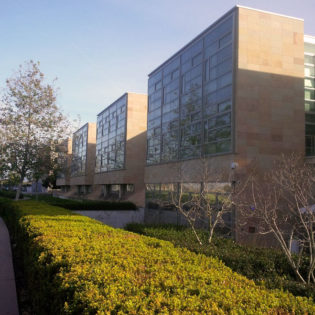
The Integrated Photonics Laboratory is located in the Engineering Sciences Building (ESB), on the main campus of the University of California Santa Barbara. It is associated with the Optoelectronics Technology Center (OTC), established by Prof. Larry Coldren. The Laboratory is equipped with state-of-the-art high-speed test and measurement systems for up to 120 Gb/s including pattern generators, arbitrary waveform generators, bit error rate testers, signal generators, network analyzers, lightwave component analyzers, optical spectrum analyzers, tunable lasers, high-speed modulators and detectors, power meters, source meters, current sources, pulse pattern generators, erbium-doped fiber amplifiers, a Raman amplifier, custom probe stations, temperature controllers, and high-speed probes. The Laboratory also houses die attach and wirebonding tools, a lapping station, and a photoluminescence (PL) measurement setup.
The iPL also manages a metalorganic chemical vapor deposition (MOCVD) system for group III-V materials including indium phosphide (InP), gallium arsenide (GaAs), and related compunds, for growth on both native substrates and on silicon. Applications include semiconductor lasers, photonic integrated circuits, nanolasers for silicon photonics, and nanoelectronics.
In addition to collaborating with several other research groups and laboratories on campus, we also utilize many of the state-of-the-art facilities available for nanofabrication and microscopy.
