Difference between revisions of "Wafer bonding"
From OptoelectronicsWiki
(→Useful references) |
|||
| (12 intermediate revisions by 6 users not shown) | |||
| Line 2: | Line 2: | ||
==Current Processes== | ==Current Processes== | ||
| − | Bonding Defects - [[Media:Bonding | + | Bonding Defects - [[Media:Bonding_Issues.pptx]] |
| + | |||
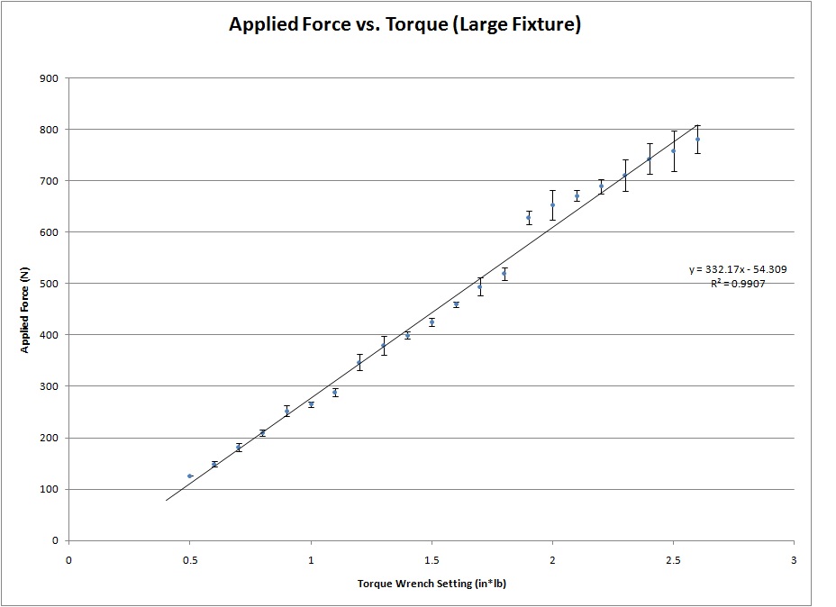
| + | Bonding Force vs. Torque wrench setting for large circular [[media:bondingfixture.jpg|bondingfixture]] | ||
| + | |||
| + | big bonding fixture: UC property tag #108000120 | ||
| + | |||
| + | ==Useful references== | ||
| + | [[Media:WIM111110-UCSB-Plasma_Activated_Bonding-new_findings-01_email.pdf| EVG]] has produced some slides on wafer bonding. Do not distribute these outside the group! | ||
| + | |||
| + | They summarize their findings on how bonding works at the molecular level. | ||
| + | Details on change in bond strength with time, use of N2 as activation, temp required for good bonding | ||
| + | and variation with presence of native oxide / thermal oxide on surface. | ||
Latest revision as of 14:22, 14 February 2012
Back to Process_Hybrid_Silicon.
Current Processes[edit]
Bonding Defects - Media:Bonding_Issues.pptx
Bonding Force vs. Torque wrench setting for large circular bondingfixture
big bonding fixture: UC property tag #108000120
Useful references[edit]
EVG has produced some slides on wafer bonding. Do not distribute these outside the group!
They summarize their findings on how bonding works at the molecular level. Details on change in bond strength with time, use of N2 as activation, temp required for good bonding and variation with presence of native oxide / thermal oxide on surface.