Difference between revisions of "DUV Stepper"
From OptoelectronicsWiki
(→Presentations) |
Jaredhulme (Talk | contribs) (→Presentations) |
||
| (19 intermediate revisions by 3 users not shown) | |||
| Line 2: | Line 2: | ||
[https://docs.google.com/spreadsheet/ccc?key=0Ai_MTssdIAw_dHY4OWRCNjY0V1MzNnFXamhVZWptN3c#gid=0 Process Follower] Google Doc | [https://docs.google.com/spreadsheet/ccc?key=0Ai_MTssdIAw_dHY4OWRCNjY0V1MzNnFXamhVZWptN3c#gid=0 Process Follower] Google Doc | ||
| + | |||
| + | ===PR etch rate=== | ||
| + | {| border="3" | ||
| + | |- style="background:green; color:white" | ||
| + | ! PR !! Equipment !! Substrate !!Recipe !! PR etch rate !! Latest update date !! Latest update by !! Calib. file !! Note | ||
| + | |- | ||
| + | | UV210 || D-RIE ||Si ||BOV_J_01||28 nm/min|| Nov 9, 2012 || Geza || - || Full 4" wafer covered in PR, ~1% Si exposed | ||
| + | |- | ||
| + | | UV210 || ICP#2 ||Si ||#101: SiOxVert||140 nm/min|| Nov 5, 2012 || Geza || - || SiO2 etch rate: 200 nm/min (?) | ||
| + | |- | ||
| + | | UV210 || ICP#2 ||Si ||#104: Nanoetch||100 nm/min|| Nov 5, 2012 || Geza || - || 5/35/5 sccm (O2/CHF3/CF4), 500/50 W, SiO2 etch rate: 100 nm/min | ||
| + | |- | ||
| + | | UV6 || ICP#2 ||Si ||#101: SiOxVert||135 nm/min|| Nov 5, 2012 || Geza || - || - | ||
| + | |- | ||
| + | | UV6 || ICP#2 ||Si ||#104: Nanoetch||90 nm/min|| Nov 5, 2012 || Geza || - || 5/35/5 sccm (O2/CHF3/CF4), 500/50 W, SiO2 etch rate: 100 nm/min | ||
| + | |- | ||
| + | | UV6 || ICP#2 ||Si ||#104: Nanoetch||145 nm/min|| Nov 5, 2012 || Geza || - || 10/35/5 sccm (O2/CHF3/CF4), 500/50 W, SiO2 etch rate: ~80 nm/min | ||
| + | |- | ||
| + | |} | ||
=== Presentations === | === Presentations === | ||
HP's development for 500 nm WGs, 200 nm coupler gaps (please don't share with people outside Bowers group): [[Media: 2012_09_11_DUV.pptx]] | HP's development for 500 nm WGs, 200 nm coupler gaps (please don't share with people outside Bowers group): [[Media: 2012_09_11_DUV.pptx]] | ||
| − | Liftoff process with negative PR (HP's work): [[Media: 2012_09_28_DUV_Liftoff.pptx]] | + | Liftoff process with positive/negative PR (HP's work): [[Media: 2012_09_28_DUV_Liftoff.pptx]] |
| − | Current Presentation: [[Media: DUV Stepper | + | Current Presentation: [[Media: DUV Stepper Waveguides_v8a.pptx]] |
Backup Presentations: [[DUV Stepper Waveguides Backup Presentations]] | Backup Presentations: [[DUV Stepper Waveguides Backup Presentations]] | ||
| Line 30: | Line 49: | ||
DUV Si 180C_0: SEMs - Gasonics x3 - Dies 25-29: [[File:180c_8_6_12.zip]] | DUV Si 180C_0: SEMs - Gasonics x3 - Dies 25-29: [[File:180c_8_6_12.zip]] | ||
| + | ====Deep Etch==== | ||
| + | DUV Si 170C_1: Post Deep Etch SEMs - E25 F-.15: [[File:11_9_12_DUV_SOI_1_DeepEtch.zip]] | ||
Return to [[Cleanroom Equipment]] | Return to [[Cleanroom Equipment]] | ||
Latest revision as of 17:17, 12 November 2012
Contents
Characterization[edit]
Process Follower Google Doc
PR etch rate[edit]
| PR | Equipment | Substrate | Recipe | PR etch rate | Latest update date | Latest update by | Calib. file | Note |
|---|---|---|---|---|---|---|---|---|
| UV210 | D-RIE | Si | BOV_J_01 | 28 nm/min | Nov 9, 2012 | Geza | - | Full 4" wafer covered in PR, ~1% Si exposed |
| UV210 | ICP#2 | Si | #101: SiOxVert | 140 nm/min | Nov 5, 2012 | Geza | - | SiO2 etch rate: 200 nm/min (?) |
| UV210 | ICP#2 | Si | #104: Nanoetch | 100 nm/min | Nov 5, 2012 | Geza | - | 5/35/5 sccm (O2/CHF3/CF4), 500/50 W, SiO2 etch rate: 100 nm/min |
| UV6 | ICP#2 | Si | #101: SiOxVert | 135 nm/min | Nov 5, 2012 | Geza | - | - |
| UV6 | ICP#2 | Si | #104: Nanoetch | 90 nm/min | Nov 5, 2012 | Geza | - | 5/35/5 sccm (O2/CHF3/CF4), 500/50 W, SiO2 etch rate: 100 nm/min |
| UV6 | ICP#2 | Si | #104: Nanoetch | 145 nm/min | Nov 5, 2012 | Geza | - | 10/35/5 sccm (O2/CHF3/CF4), 500/50 W, SiO2 etch rate: ~80 nm/min |
Presentations[edit]
HP's development for 500 nm WGs, 200 nm coupler gaps (please don't share with people outside Bowers group): Media: 2012_09_11_DUV.pptx
Liftoff process with positive/negative PR (HP's work): Media: 2012_09_28_DUV_Liftoff.pptx
Current Presentation: Media: DUV Stepper Waveguides_v8a.pptx
Backup Presentations: DUV Stepper Waveguides Backup Presentations
Pictures[edit]
160C Bake[edit]
DUV Si 160C_0 SEMs - Gasonics x3 - Dies 26-29: File:160c 8 6 12.zip
DUV Si 160C_0 Microscope Pics - After 20 min Nanostrip: File:Post 20min NanoStrip 8 10 12.zip
170C Bake[edit]
DUV Si 170C_0 SEMs - Gasonics x3 - Dies 24-27: File:170c 8 4 12.zip
DUV Si 170C_1 SEMs - PE2 2' + 1165 30' + u/s 10' + PE2 2': File:DUV-si-170C-1.zip
DUV Si 170C_2 Pic - Flood DUV pre-etch + AZ300MIF post-etch: Media:DUV_si_170C_2.jpg
DUV Si 170C_1 SEMs - Sidewall profiles post clean: File:9 7 DUV SOI 170 1 Sidewalls.zip
DUV SOI 170C_1 SEMs - 1165 30' + u/s 10' + PE2 2': File:8 28 DUV SOI 170C 1.zip
DUV SOI 170C_1 SEMs - 1165 30' + u/s 10' + PE2 2': File:8 31 DUV SOI 170C 1.zip
DUV SOI 170C_1 SEMs - ZigZag Grating: File:9 11duvzigzaggrating.zip
180C Bake[edit]
DUV Si 180C_0: SEMs - Gasonics x3 - Dies 19-28: File:180c 8 4 12.zip
DUV Si 180C_0: SEMs - Gasonics x3 - Dies 25-29: File:180c 8 6 12.zip
Deep Etch[edit]
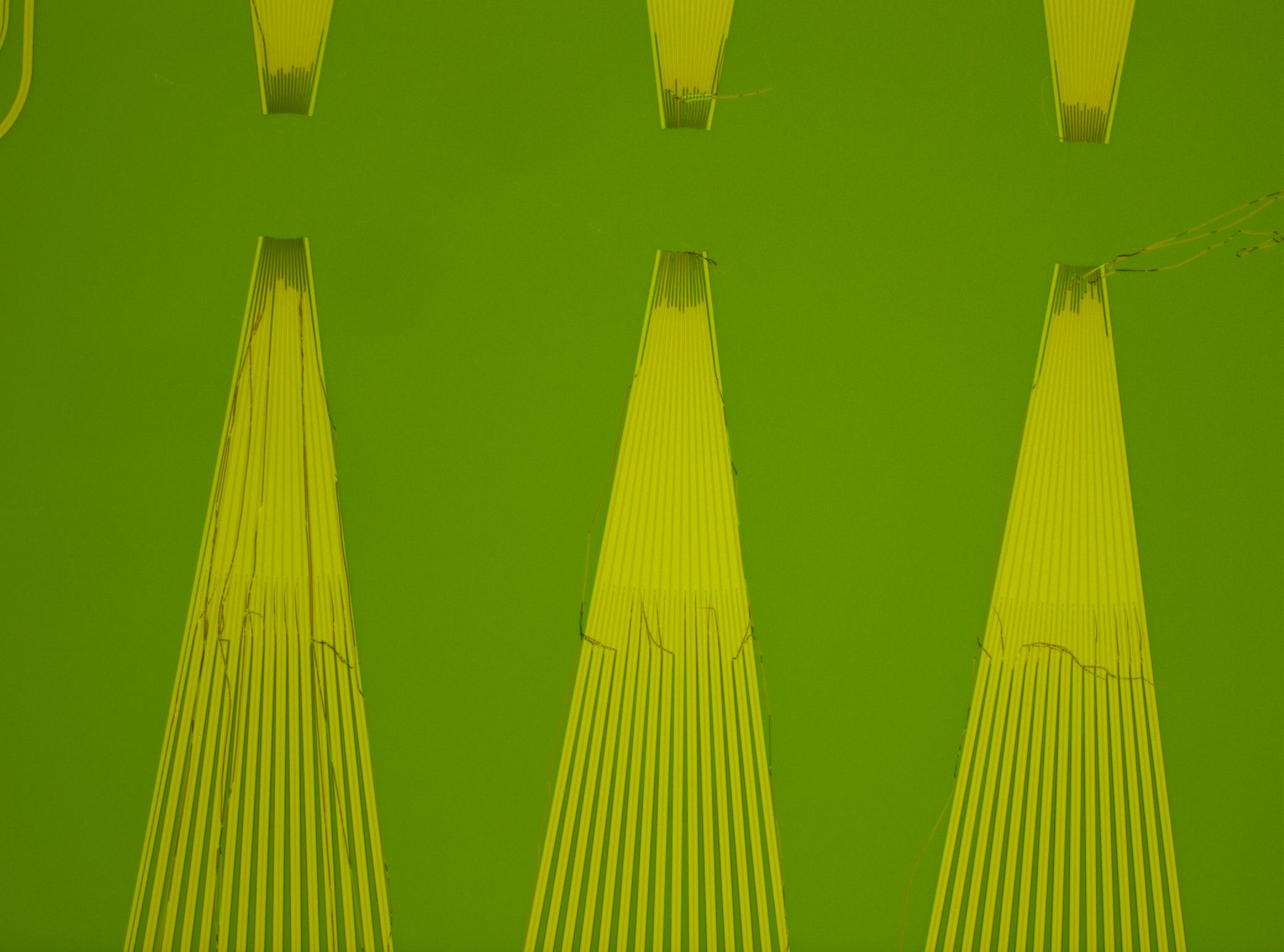
DUV Si 170C_1: Post Deep Etch SEMs - E25 F-.15: File:11 9 12 DUV SOI 1 DeepEtch.zip
Return to Cleanroom Equipment