Lab and Center Spotlights — Electronics & Photonics
Quantum Photonics Lab (QPL)
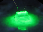
Galan Moody
Research Center Spotlight — Solid-State Lighting and Energy Electronics Center (SSLEEC)
Palmstrøm Research Group
Chris Palmstrøm
Nanophotonics Research Group
Jon Schuller
Optoelectronics Research Group
John Bowers
Photonic Devices and Integrated Circuits Laboratory
Nadir Dagli
Quantum Photonics Lab (QPL)
Galan Moody
 In the lab we develop nanophotonic and optoelectronic technologies to advance our understanding of quantum light-matter interaction for a wide range of applications – from novel computing architectures to communications, sensing, and emerging fields such as valleytronics.
We address important challenges in these areas through the discovery of new quantum materials and nanostructures, interfacing them with photonic, optoelectronic, and optomechanical devices based on fundamentally new concepts and prototypes, and developing innovative quantum-limited measurement tools. We are motivated by questions such as
- How can we engineer programmable solid-state quantum systems that are optimally suited for specific tasks in computing and communications?
- What quantum advantages arise by interfacing different physical systems into a monolithic, hybrid platform?
- What are the fundamental limitations to manipulating, distributing, and storing quantum information across different physical systems?
To answer these questions, our lab specializes in a broad range of platforms including III-V quantum dots, 2D materials and heterostructures, and the fabrication of photonic, optoelectronic, and optomechanical devices. For each project, we also explore emergent properties by combining multiple materials and systems into a hybrid platform using heterogeneous integration methods.
Reseearch Areas
 Integrated Quantum Photonic Circuits: Optical technologies for quantum cryptography, communications, and computing that exhibit size, weight, and power (SWaP) advantages over classical machines benefit from reducing existing table-top optical systems to all-on-chip photonic circuits. We utilize a heterogeneous approach that combines state-of-the-art quantum light sources based on III-V and 2D material quantum emitters with silicon-based photonics and superconducting nanowire single-photon detectors to realize fully integrated chip-scale quantum photonic circuits.
 Hybrid Quantum Systems and Networking: Interfacing different quantum systems into a monolithic, hybrid platform is a promising direction for achieving new functionality and scalability for distributed computing and networking. We explore the exchange, distribution, and storage of quantum information between dissimilar quantum systems spanning microwave-to-optical frequency scales, such as superconducting circuits, quantum acoustic cavities and waveguides, and solid-state quantum emitters.
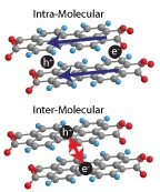
  2D Material Photonics and Valleytronics: The ability to engineer the optical and electronic properties of nanoscale materials layer-by-layer and atom-by-atom is now a reality due to the recent discoveries of a large class of atomically thin 2D materials, including graphene, transition metal dichalcogenides, and hexagonal boron nitride. We fabricate and study heterostructures of these materials and examine how their integration with photonic, optoelectronic, and optomechanical devices can be utilized in quantum information processing, communications, and valleytronics.
Professor Moody's:
Solid-State Lighting and Energy Electronics Center (SSLEEC)
SSLEEC is a collaborative center, which partners key industry leaders and UCSB researchers to advance solid-state lighting and energy efficient power switching using wide-bandgap semiconductors. The Center is focused on new semiconductor-based technologies for energy efficient lighting, power electronics, and bulk growth of Gallium Nitride (GaN).
MAIN RESEARCH AREAS:
High Efficiency LEDs for Lighting and Displays
- UV, blue, green, yellow, and red
- Advanced epitaxial growth
- Low defect density substrate growth
- Advanced packaging for light extraction
- Micro-LED development for mobile displays
Laser-Based Lighting
- Blue (415-450 nm) and green (525 nm) high-power laser diodes
- Novel phosphor materials and matrices for high-power applications
- Compact, high-brightness, high-efficiency, directional sources
Power Electronics using AlGaN/GaN (98% efficient > 2kV)
- High breakdown voltage
- Low on resistance
- Vertical transistors
Bulk Crystal Growth
- Low cost bulk GaN
- Ammonothermal growth of bulk GaN
CENTER & LEADERSHIP:
- Solid-State Lighting and Energy Electronics Center (SSLEEC)
- Steven DenBaars (Materials/ECE), Shuji Nakamura (Materials/ECE), Umesh Mishra (ECE), James Speck (Materials) and Chris Van de Walle (Materials)
Palmstrøm Research Group
Chris Palmstrøm
The general research interests of the group are on the heteroepitaxial growth of novel materials and structures to form the basis for making new electronic, optoelectronic, magnetic and micromechanical devices. Critical to the advancement of materials and structures is the fundamental understanding of growth. A key to developing structures with novel properties is the ability to control, at the atomic level, the interface structure and chemistry.
The program has a strong emphasis on heteroepitaxial growth of dissimilar materials. These include materials with different crystal structure, bonding, electronic, optical and magnetic properties.
Palmstrøm Group — Areas of Research
 Low Dimensional Semiconductors: their application in the study of mesoscopic phenomena and in quantum information processing has cemented low-dimensional semiconductors at the forefront condensed matter and materials physics research.
 Heusler Alloys: focuses on the growth of Heusler compounds by molecular beam epitaxy and characterization of their atomic, electronic, and magnetic properties. Examples include the half metal Co2MnSi, the semiconductors NiTiSn and CoTiSb, and the shape memory alloy Ni2MnGa.
 Spintronics: studies the fundametals
of spin transport, including spin injection
into semiconductors, spin transport in semiconductors, and spin valve and
spin torque related effects in magnetoresistive device.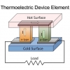 Thermoelectrics and Self Assembled Nanostructures: research is in two promising classes of thermoelectric materials for increasing the efficiency of thermoelectric devices: (i) Epitaxial III-V based nanocomposites and (ii) Semiconducting half-Heusler alloys.
 Oxides: the ability to grow thin film heterostructures of Oxide materials, with techniques such as MBE, has resulted in a wealth of new material properties not seen in the bulk state.
Professor Palmstrøm's:
Nanophotonics Research Group
Jon Schuller
At a fundamental level, our research concerns novel physical phenomena that occur when light interacts with objects of subwavelength dimensions. As engineers, we exploit these discoveries to make smaller, faster, and more efficient photonics technologies. The essential constituents of these investigations are individual subwavelength elements we refer to as “optical antennas”.
We are particularly interested in antenna-like effects arising from oriented multipolar resonances in dielectric and molecular constituents. We study how these effects lead to novel optical properties in engineered metamaterials and organic semiconductors respectively. We use engineered nanoantennas as model systems for understanding and influencing electromagnetic phenomena in atoms and molecules. Ultimately, we hope this research will lead to a future where optical properties are controlled and engineered at the atomic or molecular level.
Our research comprises investigations in the following areas:
- Plasmonics
- Metamaterials
- Thermal Emitters
- Optical Forces
- Optical Properties of Organics
- Nanophotonic Solar Cell Architectures
Professor Schuller's:
Optoelectronics Research Group
John Bowers
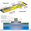
The Bowers group develops new optoelectronic components and photonic integrated circuits (PICs) for advanced fiber optic communications networks and optical interconnects. Our focus is on integrating optimum waveguiding materials, which do not interact strongly with light, with materials better-suited for active components. Most of this research falls into one of the following two areas:
- Silicon photonics: the hybrid silicon photonic platform combines the optical properties of III-V materials and germanium with the low material loss and low cost of silicon. Our group has demonstrated high-performance components such as continuous-wave and mode-locked lasers, 40Gb/s Mach-Zehnder and 50Gb/s electroabsorption modulators, and high-speed photodetectors, as well as more complex photonic integrated circuits: optical buffers, tunable microwave filters, a laser-modulator array, and a triplexer
- Silica-based platform: ultra-low loss waveguides have applications in PICs that require long delay lines, such as optical gyroscopes on a chip, optical buffers, true-time delays, and stable and narrow-linewidth microwave and optical sources. The group uses high aspect ratio Si3N4 waveguides to achieve record low loss
Our group also explores ways to efficiently convert heat and light into energy:
- Thermoelectrics: our lab is developing and characterizing novel III-V compound and Si-based nanostructured thermoelectric materials. We work both on optimizing the material power conversion efficiency and characterizing thermal and electrical properties of thin-films and challenging structures
- Photovoltaics: our research focuses on combining various materials to further enhance multi-junction solar cell efficiency
Professor Bowers':
Photonic Devices and Integrated Circuits Laboratory
Nadir Dagli
Research Focus
- Design, fabrication and modeling of guided-wave components for photonic integrated circuits
- Ultra fast, ultra low drive voltage electro-optic compound semiconductor optical modulators
- WDM components
- Advanced novel processing techniques
- Photonic nanostructures
Professor Dagli's:
Integrated Photonics Laboratory
Jonathan Klamkin
RF & Mixed-signal Integrated Systems Laboratory
Jim Buckwalter
Optical Communications and Photonic Networks Group
Dan Blumenthal
Optoelectronics Technology Center
Larry Coldren
High Frequency Electronics Group
Mark Rodwell
Integrated Photonics Laboratory (iPL)
Jonathan Klamkin
Integrated photonics greatly reduces the size, weight, and power (SWaP) while improving performance and reliability of photonic systems. The iPL pioneers integrated photonic technologies for a diverse set of applications including:
- free space optical communications
- optical interconnects in data center networks and high-performance computers
- microwave photonics and millimeter wave (mmW) communications, sensing, and visible light communications or Lifi
Our mission is to develop novel materials, devices and photonic integrated circuits (PICs) to enable systems that are beneficial to society.
Photonic Technologies
Our group has developed expertise in a broad range of photonic technology platforms including the compound semiconductors indium phosphide (InP) and gallium arsenide (GaAs), silicon photonics (SiPh), and planar lightwave circuit (PLC) such as silica, alumina, and silicon nitride. For each application or project, we apply the most suitable technology. We also oftentimes merge more than one technology with hybrid and heterogeneous integration techniques.
 Research Areas
- Free Space Optical Communications: Integrated photonics is ideal for deploying low SWaP photonic systems for space exploration and for delivering broadband connectivity to remote locations
- Microwave Photonics: This is where RF engineering meets optoelectronics. Microwave photonics requires high-performance active devices (ex. lasers, photodetectors, modulators) and novel functionality (ex. integrated true time delay, lattice filters)
- Optical Interconnects: Data centers, high-performance computers, and networks on chip (NoCs) require low-power optical interconnects and architecture design optimization
- Integrated Nanophotonics: Novel materials such as graphene and indium tin oxide (ITO) demonstrate unique optoelectronic properties for compact devices such as optical modulators and switches
- 3D Integrated Silicon Photonics: Laser and interposer integration will be crucial for realizing a truly manufacturable SiPh platform
- Visible Light Communications: Solid state lighting will reduce global energy consumption but also offer a platform to create intelligent lighting systems. These demand advanced visible light sensors
Professor Klamkin's:
RF & Mixed-signal Integrated Systems Laboratory
Jim Buckwalter
 RF Circuits for Reconfigurable Radios
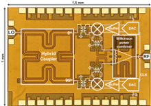
We as a society demand wireless mobility. As more devices share the same spectrum (e.g. WiFi, Bluetooth, cellular), the result is a radio-frequency traffic jam. This congestion has spurred interest in next generation –5G – access technologies. Solutions to RF spectrum congestion require transformative approaches to radio design and spectrum access. Two potential solutions include finding new spectrum or developing cognitive radio techniques for collaborating within the existing congested spectrum. One proposal to find new spectrum is to exploit microwave and millimeter-wave frequency bands where 50 times the bandwidth is available compared to current RF bands, allowing for a substantial increase in the data rate of wireless networks.
Professor Buckwalter is investigating several solutions for future wireless networks including millimeter-wave transmitter and receiver circuitry, phased array systems for beamforming, and software defined techniques for transmitter and receiver. By using highly-scaled (nanometer) CMOS IC technologies, our group investigates new circuit and system approaches that leverage electromagnetics, analog circuitry, digital signal processing, and device physics. We seek to understand the fundamental limits of communication through the implementation of integrated circuits and systems.
To learn more Prof. Buckwalter's research, see his group website.
Professor Buckwalter's:
Optical Communications and Photonic Integration (OCPI)
Dan Blumenthal
The Blumenthal Group’s research includes systems level photonic networks, photonic integrated circuits, and low loss waveguides.
- Label Switched Optical Router (LASOR)
The current bottleneck in high-speed optical communications is the high speed electronics required to process 40 Gb/s signals. This is due to the current OEO conversion - converting the optics into high-speed electronics, performing all the routing and buffering decisions, then converting back into the optical domain by modulating a fiber-coupled laser. An integral concept of the LASOR project is that we only convert a much lower bit rate "label" into the electrical domain, allowing the 40 Gbps "payload" to remain in the optical domain. The 10 Gbps header information contains routing information for the physical layer optical network, and is deserialized and processed using 156.25 MHz FPGA boards to provide appropriate electrical signals for the PFCs (Packet Forwarding Chips) and Buffer chips, which then physically route and synchronize the data.
- Terabit/s Coherent OTDM Transmission System
In fiber-optic communications, optical time-division multiplexing (OTDM) technique aggregates large capacity on a single optical wavelength. Traditional OTDM system encodes data with a simple binary power level scheme, namely on-off keying (OOK). This research explores ways of incorporating OTDM with coherent optical communication technique, which encodes data with multi-level amplitude and phase of optical wave, therefore increases the single wavelength capacity beyond Terabit/s without expanding the optical bandwidth.
- InP Photonic Integrated Circuits (PICs):
A wide variety of PICs have been developed on InP, including wavelength converters, packet forwarding chips for optical packet switched networks, mode-locked lasers for clock recovery and retiming applications, lasers with sub-wavelength metal gratings, coherent receivers, all-optical regenerators.
- Ultra-Low-Loss Waveguides and Applications
We design and fabricate ultra low loss waveguides on a Si3N4/SiO2 platform. Record low loss has been achieved, which allows for the integration of optical delay lines with lengths not previously feasible on a chip scale. With this new platform developed, many applications are now being studied where long delay line can be of great impact. Some of the applications currently under study are: true time delays for phased array antennas in microwave photonics, optical gyroscopes, narrow linewidth lasers, and optical buffering.
Professor Blumenthal's:
Optoelectronics Technology Center
Larry Coldren
It is widely recognized that technologies that can intelligently manipulate light (photons) is the key to addressing current and future challenges in communications. Our research group is poised to meet these challenges by developing highly-functional photonic integrated circuits (PICs) and efficient high-speed vertical cavity surface emitting lasers (VCSELs) for advanced fiber optic communications and sensor networks as well as for use in optical interconnects.
Our PICs have demonstrated mode and phase locking, programmability in amplitude, phase and wavelength as well as electro-optic beam steering -- all in a monolithically integrated platform. Our recent work on VCSELs have led to devices that operate >35 Gb/s while using only 286 fJ/bit, and more recently, the first demonstration of gain modulation in a VCSEL using carrier separation as well as high extinction polarization-switching VCSELs.
We focus on all aspects of the design process from simulation and epitaxial design to fabrication and system testing. In addition, our capability of growing high quality GaAs, and InP based material in-house gives us a unique perspective in our research.
Areas of Interest:
- High-performance photonic integrated circuits (PICs): PICs incorporate active gain regions together with other waveguide elements, such as splitters, reflectors, modulators and detectors, in a compatible guided wave technology to produce highly versatile optical circuits on-chip. Some devices, such as optical phase-locked loops, require such short feedback delays require integration. Others devices, such as tunable lasers, wavelength converters, and tunable filters, benefit from the stability and great tolerance to noise, achieved by integration. Recently, we have demonstrated fully integrated optical phase-locked loops, homodyne coherent receivers, programmable active optical-filters, broadband mode-locked lasers, and electro-optical beam steering.
- Vertical Cavity Surface Emitting Lasers: Compact, efficient and capable of direct high-speed modulation, VCSELs are great sources for active cables and highly-efficient optical interconnects. Our group has developed VCSELs that can support data rates > 35Gbps with the highest energy efficiency value of 286 fJ/bit for a 980 nm wavelength. Methods for enhancing the active region through precise doping and highly-strained quantum wells are currently being explored. A novel three-terminal VCSEL was also developed in our group that demonstrated for the first time in a VCSEL structure gain-modulation through carrier separation. In another unique design, we demonstrated the ability to switch output polarization of a VCSEL through asymmetric current injection.
Professor Coldren's:
High Frequency Electronics Group
Mark Rodwell
Our research focuses on nm and high-frequency electronics. Our Ph.D. students are active in developing nm transistors for VLSI, and developing
THz transistors, designing silicon and III-V integrated circuits, and demonstrating systems for mm-wave and THz wireless communications and radar.
Professor Rodwell's: