Difference between revisions of "SWEEPER"
(→Characterization) |
(→Characterization) |
||
| Line 65: | Line 65: | ||
== Characterization == | == Characterization == | ||
<u><b>Hybrid SI Tunable Laser re-RUN - Sweeper 4.1</b></u> <br> | <u><b>Hybrid SI Tunable Laser re-RUN - Sweeper 4.1</b></u> <br> | ||
| − | '''Run 4.1''' | + | '''Run 4.1'''<br> |
| − | Post Bond ''Macroscopic'' Pictures - Samples H,I,J,K - [[File:SW4_1_PostBond+100nmOxide_Macroscopic.zip]] | + | Post Bond ''Macroscopic'' Pictures - Samples H,I,J,K - [[File:SW4_1_PostBond+100nmOxide_Macroscopic.zip]]<br> |
| − | Post Bond ''Microscopic'' Pictures - Samples H,I,J,K - [[File:SW4_1_PostBond+100nmOxide_Microscopic.zip]] | + | Post Bond ''Microscopic'' Pictures - Samples H,I,J,K - [[File:SW4_1_PostBond+100nmOxide_Microscopic.zip]]<br> |
| − | PMesa Etch Rie 2 traces - [[File:SW4_1_MesaEtch_Rie2Traces.zip]] | + | PMesa Etch Rie 2 traces - [[File:SW4_1_MesaEtch_Rie2Traces.zip]]<br> |
| − | PMesa Etch SEMs - [[File:PMEtch.zip]] | + | PMesa Etch SEMs - [[File:PMEtch.zip]]<br> |
| − | QW Etch SEMs - [[File:QWetch.zip]] - Shows roughness of RIE2 etch vs the smoothness of the wet etch | + | QW Etch SEMs - [[File:QWetch.zip]] - Shows roughness of RIE2 etch vs the smoothness of the wet etch<br> |
| − | NMetal Litho Pictures - Samples I - [[File:nmetallithochipi.zip]] | + | NMetal Litho Pictures - Samples I - [[File:nmetallithochipi.zip]]<br> |
| − | NMetal Liftoff Pictures - Samples I,J,K - [[File:nmetalliftoff.zip]] - Shows stringers, bubbles, failed liftoff, uneven RIE2 etch(?) in certain areas. | + | NMetal Liftoff Pictures - Samples I,J,K - [[File:nmetalliftoff.zip]] - Shows stringers, bubbles, failed liftoff, uneven RIE2 etch(?) in certain areas.<br> |
| − | N-InP Etch Picture - Samples K - [[Media:NInP_Etch_K_1.png]] | + | N-InP Etch Picture - Samples K - [[Media:NInP_Etch_K_1.png]]<br> |
| − | VIA1 Litho - Sample K - [[File:Via1Litho_K_R1C1.zip]] - Shows how mesa pattern is compressed with respect to Via1 pattern. | + | VIA1 Litho - Sample K - [[File:Via1Litho_K_R1C1.zip]] - Shows how mesa pattern is compressed with respect to Via1 pattern.<br> |
| − | VIA1 etch AFM results - [[File:AFM after via etch analyzed.zip]] | + | VIA1 etch AFM results - [[File:AFM after via etch analyzed.zip]]<br> |
| − | VIA1 Blanket etch Dektaks - [[File:Via_Blanket_Etch_Dektaks.zip]] | + | VIA1 Blanket etch Dektaks - [[File:Via_Blanket_Etch_Dektaks.zip]]<br> |
| − | ThermoOptic Metal Litho - [[File:ToMetLitho.zip]] | + | ThermoOptic Metal Litho - [[File:ToMetLitho.zip]]<br> |
| − | Post Via2 Etch Strip Stringers - [[File:Post Via2 Etch Strip Stringers.zip]] | + | Post Via2 Etch Strip Stringers - [[File:Post Via2 Etch Strip Stringers.zip]]<br> |
| − | Post Via2 Litho Cracking - [[File:PostVia2LithoCracking.zip]] | + | Post Via2 Litho Cracking - [[File:PostVia2LithoCracking.zip]]<br> |
| − | Post-Unaxis-Oxide-Deposition Failed Photoresist Spin - [[Media:J_badPRspin.jpg]] - Recipe Barton_SiO2_50C. Solution: solvent clean, dehydration bake, 2 min PEII at 200W | + | Post-Unaxis-Oxide-Deposition Failed Photoresist Spin - [[Media:J_badPRspin.jpg]] - Recipe Barton_SiO2_50C. Solution: solvent clean, dehydration bake, 2 min PEII at 200W<br> |
| − | IVs spot Check 1_28_13 - [[File:IVs - Preliminary - 1_28_13.zip]] | + | IVs spot Check 1_28_13 - [[File:IVs - Preliminary - 1_28_13.zip]]<br> |
| − | LIVs 2_1_13 - [[File:LIVs - 2_1_13.zip]] | + | LIVs 2_1_13 - [[File:LIVs - 2_1_13.zip]]<br> |
| − | LIVs 2_4_13 - [[File:LIVs - 2_4_13.zip]] | + | LIVs 2_4_13 - [[File:LIVs - 2_4_13.zip]]<br> |
| − | '''LIVs in Excel - SGDBR 29 Lasers found - [[File:LIVs_Excel.zip]]''' | + | '''LIVs in Excel - SGDBR 29 Lasers found - [[File:LIVs_Excel.zip]]'''<br> |
| − | '''Chip K - Vernier 05 - LIV and OSA data - [[File:K_R1C2_Vernier05.xlsx]]''' | + | '''Chip K - Vernier 05 - LIV and OSA data - [[File:K_R1C2_Vernier05.xlsx]]'''<br> |
| − | <br><br><br> | + | <br><br> |
<u><b>aSI PHASE MODULATOR RUN - Sweeper 3.1</b></u> <br> | <u><b>aSI PHASE MODULATOR RUN - Sweeper 3.1</b></u> <br> | ||
'''Run 1''' | '''Run 1''' | ||
| − | Step - Description - Sample Names - File | + | Step - Description - Sample Names - File<br> |
| − | 3.3 - Rib litho pics before hard mask etch: [[File:rib litho pics.zip]] | + | 3.3 - Rib litho pics before hard mask etch: [[File:rib litho pics.zip]]<br> |
| − | 3.4 - Rib Pics before Si Etch - Dummy 1 : [[File:dummy_post_pr_strip_pre_rib_etch.zip]] | + | 3.4 - Rib Pics before Si Etch - Dummy 1 : [[File:dummy_post_pr_strip_pre_rib_etch.zip]]<br> |
| − | 3.4 - Rib Pics before Si Etch - Sample 1: [[File:sample1_pre_si_etch.zip]] | + | 3.4 - Rib Pics before Si Etch - Sample 1: [[File:sample1_pre_si_etch.zip]]<br> |
| − | 3.4 - Rib Pics before Si Etch - Sample 2: [[File:sample2_pre_si_etch.zip]] | + | 3.4 - Rib Pics before Si Etch - Sample 2: [[File:sample2_pre_si_etch.zip]]<br> |
| − | 3.5 - Rib Pics post Si Etch - Sample 2: [[File:sample2_post_si_etch.zip]] | + | 3.5 - Rib Pics post Si Etch - Sample 2: [[File:sample2_post_si_etch.zip]]<br> |
'''Run 2''' | '''Run 2''' | ||
| − | [[File:P1vid.zip]] | + | [[File:P1vid.zip]]<br> |
| − | Step - Description - Sample Names - File | + | Step - Description - Sample Names - File<br> |
| − | 3.5 - SEM post Si Etch - Dummy 2: [[File:Dummy2_SEM_post_si_etch.zip]] | + | 3.5 - SEM post Si Etch - Dummy 2: [[File:Dummy2_SEM_post_si_etch.zip]]<br> |
| − | 4.4 - N-Dope Litho (Implant 3A) - Sample 3 & 4: [[File:ndopelithopics.zip]] | + | 4.4 - N-Dope Litho (Implant 3A) - Sample 3 & 4: [[File:ndopelithopics.zip]]<br> |
| − | 4.5 - Post Implant 3A PR Strip - Sample 3 & 4: [[File:post_imp3A_PR_strip.zip]] | + | 4.5 - Post Implant 3A PR Strip - Sample 3 & 4: [[File:post_imp3A_PR_strip.zip]]<br> |
| − | 5.3 - P-Dope1 Litho (Implant 3B) - Sample 3 & 4: [[File:implant3B_litho.zip]] | + | 5.3 - P-Dope1 Litho (Implant 3B) - Sample 3 & 4: [[File:implant3B_litho.zip]]<br> |
| − | 5.4 - Post Implant 3B PR Strip: [[Media:post_imp3B_PR_strip.jpg]] | + | 5.4 - Post Implant 3B PR Strip: [[Media:post_imp3B_PR_strip.jpg]]<br> |
| − | 6.3 - P-Dope2 Litho (Implant 3C) - Sample 3 & 4: [[File:implant3C_litho.zip]] | + | 6.3 - P-Dope2 Litho (Implant 3C) - Sample 3 & 4: [[File:implant3C_litho.zip]]<br> |
| − | 6.4 - Post Implant 3C Partial PR Strip, "Cracks" - S3_Dies 1,2: [[File:Cracking_Pics_post_3C_Strip_1.jpg]] | + | 6.4 - Post Implant 3C Partial PR Strip, "Cracks" - S3_Dies 1,2: [[File:Cracking_Pics_post_3C_Strip_1.jpg]]<br> |
| − | 7.1 - Post 1050C Anneal (S3 and Dum2 taken to unknown temp): [[File:post_1050C_anneal_pics.zip]] | + | 7.1 - Post 1050C Anneal (S3 and Dum2 taken to unknown temp): [[File:post_1050C_anneal_pics.zip]]<br> |
| − | 9.2 - Via 1 Litho - Dum2, S3, S4: [[File:Via_1_litho_pics.zip]] | + | 9.2 - Via 1 Litho - Dum2, S3, S4: [[File:Via_1_litho_pics.zip]]<br> |
| − | 9.4 - Via 1 Etched, PR Stripped: [[File:Via1_Etch_PR_Stripped.zip]] | + | 9.4 - Via 1 Etched, PR Stripped: [[File:Via1_Etch_PR_Stripped.zip]]<br> |
| − | 10.1 - Failed Contact (NMetal) Litho - Dum2, S3, S4: [[File:failed_contact_Litho.zip]] | + | 10.1 - Failed Contact (NMetal) Litho - Dum2, S3, S4: [[File:failed_contact_Litho.zip]] <br> |
| − | 10.1 - Contact (NMetal) Litho - [[File:NMetal Litho.zip]] | + | 10.1 - Contact (NMetal) Litho - [[File:NMetal Litho.zip]]<br> |
| − | 10.3 - Contact Metal Liftoff - [[File:Liftoff Results.zip]] | + | 10.3 - Contact Metal Liftoff - [[File:Liftoff Results.zip]]<br> |
| − | 12.2 - Via 2 Litho - [[File:Via2Litho.zip]] | + | 12.2 - Via 2 Litho - [[File:Via2Litho.zip]]<br> |
| − | 12.3 - Post 5 & 10 min SU8 etch - [[File:post5and10minetchsu8.zip]] | + | 12.3 - Post 5 & 10 min SU8 etch - [[File:post5and10minetchsu8.zip]]<br> |
| − | 12.. - SU8 Removal - SiNetch 2.5' + SU8 etch 3.5'+3.5' + ISO u/s 5' + Piranha 1' - [[File:su8removalpostpiranhadip.zip]] | + | 12.. - SU8 Removal - SiNetch 2.5' + SU8 etch 3.5'+3.5' + ISO u/s 5' + Piranha 1' - [[File:su8removalpostpiranhadip.zip]]<br> |
| − | 13.1 - SU8 Swabbed off/ PRMetal Litho - Sample 4 - [[File:SwabbingSU8_&_ProbeMetalLitho.zip]] | + | 13.1 - SU8 Swabbed off/ PRMetal Litho - Sample 4 - [[File:SwabbingSU8_&_ProbeMetalLitho.zip]]<br> |
| − | 13.4 - 2nd PRMetal Layer Lifted off - Sample 4 - [[File:2nd PRMetal Layer 9_5_12.zip]] | + | 13.4 - 2nd PRMetal Layer Lifted off - Sample 4 - [[File:2nd PRMetal Layer 9_5_12.zip]]<br> |
| − | 14.4 - Post Grating Opening Etch/Strip - Sample 4 - [[File:9_7postGOstrip.zip]] | + | 14.4 - Post Grating Opening Etch/Strip - Sample 4 - [[File:9_7postGOstrip.zip]]<br> |
<u><b>PASSIVES RUN</b></u> <br> | <u><b>PASSIVES RUN</b></u> <br> | ||
Passive grating results: [[File:sweeper_Q2.doc]] <br> | Passive grating results: [[File:sweeper_Q2.doc]] <br> | ||
2D beam steering results, OFC video: [[File:OFC_Doylend_vid2.zip]] | 2D beam steering results, OFC video: [[File:OFC_Doylend_vid2.zip]] | ||
Revision as of 12:02, 8 April 2013
Overview
SWEEPER, formally known as "Chip-scale Integrated Photonic Phased Array" (CHIPPA) aims to produce a phased array of waveguide-coupled surface gratings integrated with an on-chip tunable laser, amplifiers, and phase modulators for free-space beam control in 2 axes.
Simulations
Run 2 current injection modulator:
Processing
RUN 5.A (SWEEPER Phase II 32x Si PIC)
Process overview: File:SWEEPER5A v03.ppt
Process traveller: File:SWEEPER5 Trav-v01.docx
Google docs traveller (shows real-time results and progress):
Previous traveller:
Mask set: File:SWEEPER5.zip
RUN 4.1 (Hybrid Silicon only for tunable lasers)
Process overview: File:SWEEPER4-1 v4.ppt
Process traveller: File:SWEEPER HSi-Trav31.0 Run4.1.docx
Google docs traveller (shows real-time results and progress): [1]
Previous traveller: File:SWEEPER HSi-Trav30.2 Run4.1.docx
Mask set: File:SWEEPER4.zip
RUN 3.2 (Hybrid Silicon only for SOA tests)
(combined with EPHI Dev2 Run)
RUN 3.1 (active Silicon only for fast phase modulator tests)
Media:SWEEPER_3.1_Gratings.zip
Current Traveler for ACTIVES Run 3 - Phase modulator run: Media:SWEEPER Actives Trav v21_2b ACTIVE SI ONLY.docx <-- note the new dopant anneal recipe: 5mins instead of 10.
Old Traveler for ACTIVES Run 3 - Phase modulator run: Media:SWEEPER Actives Trav v21_1 ACTIVE SI ONLY.docx
Powerpoint overview (trav 21_2): Media:process flow SWEEPER RUN3_1 trav v21_2.pptx
Planned schedule for ACTIVES Run 3 - Phase modulator run: aSi-PM Process Schedule
Mask set: Media:SWEEPER 3_1 - aSi Shortloop v12.zip
Mask set showing EBL layer: Media:SWEEPER 3_1 - aSi_Shortloop_v12B (EBL incl).zip (top cell is AAA_aSi_FULL_FLAT)
Chip status is maintained on a google doc: Google doc traveller
Current Anneal Recipes for ACTIVES Run 1:: Media:Sweeper_Anneal_Recipe.xlsx
RUN 2.4 (hybrid Silicon only for Phase 1 tunable lasers retest)
Traveler: Media:SWEEPER_MDHybrid_Trav_v02_HYBRID_SI_ONLY.docx
Mask set through EBL: Media:SWP_2-4_WG2-VC-EBL.zip
RUN 2.3 (hybrid Silicon only for Phase 1 tunable lasers test)
Traveler used for ACTIVES Run 1A (hybrid silicon only - no active silicon): Media:SWEEPER Actives Trav vH20_2_HYBRID-ONLY.docx
RUN 2.2 (both active and hybrid Silicon for Phase 1 PIC)
Traveler used for ACTIVES Run 1 (full process, chips A-E, produced chips A2, E1, E2): Media:SWEEPER Actives Trav v20_1.docx
Mask used for ACTIVES Run 1: Media:SWEEPER_ACTIVES85_TAPEDOUT.zip
RUN 2.1 (active Silicon for Phase 1 intermediate testing)
Prior traveler for ACTIVES Run 1 (active Si only): Media:SWEEPER Actives Trav v15_3.xls
RUN 1.2(spring/summer 2011 - passive SWEEPER for Phase 1 with revisions to avoid grating damage)
Traveler for Run 2B: Media:110202 Sweeper Rev1.1 Run 2B.xls
RUN 1.1(early spring 2011 - passive SWEEPER for Phase 1)
Traveler for Run 1: Media:110202_Sweeper_Rev1_Batch_1.xls
Powerpoint overview can be found here Media:SWEEPER_process_flow.pptx
Prelim mask:
File:SWEEPER ACTIVES55 semifinal flat2.cif
File:SWEEPER ACTIVES59 semifinal flat2.cif
Grating Reports:
Media:Sweeper_Run_2B_-_GratingReport-2.pptx
Characterization
Hybrid SI Tunable Laser re-RUN - Sweeper 4.1
Run 4.1
Post Bond Macroscopic Pictures - Samples H,I,J,K - File:SW4 1 PostBond+100nmOxide Macroscopic.zip
Post Bond Microscopic Pictures - Samples H,I,J,K - File:SW4 1 PostBond+100nmOxide Microscopic.zip
PMesa Etch Rie 2 traces - File:SW4 1 MesaEtch Rie2Traces.zip
PMesa Etch SEMs - File:PMEtch.zip
QW Etch SEMs - File:QWetch.zip - Shows roughness of RIE2 etch vs the smoothness of the wet etch
NMetal Litho Pictures - Samples I - File:Nmetallithochipi.zip
NMetal Liftoff Pictures - Samples I,J,K - File:Nmetalliftoff.zip - Shows stringers, bubbles, failed liftoff, uneven RIE2 etch(?) in certain areas.
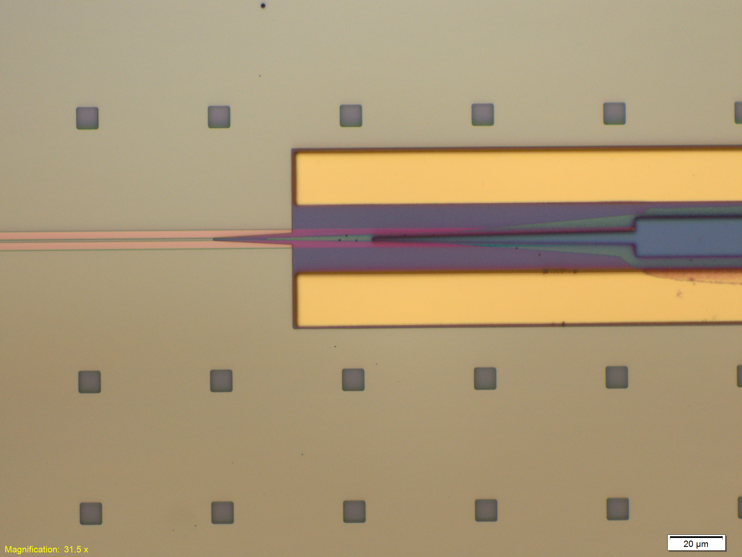
N-InP Etch Picture - Samples K - Media:NInP_Etch_K_1.png
VIA1 Litho - Sample K - File:Via1Litho K R1C1.zip - Shows how mesa pattern is compressed with respect to Via1 pattern.
VIA1 etch AFM results - File:AFM after via etch analyzed.zip
VIA1 Blanket etch Dektaks - File:Via Blanket Etch Dektaks.zip
ThermoOptic Metal Litho - File:ToMetLitho.zip
Post Via2 Etch Strip Stringers - File:Post Via2 Etch Strip Stringers.zip
Post Via2 Litho Cracking - File:PostVia2LithoCracking.zip
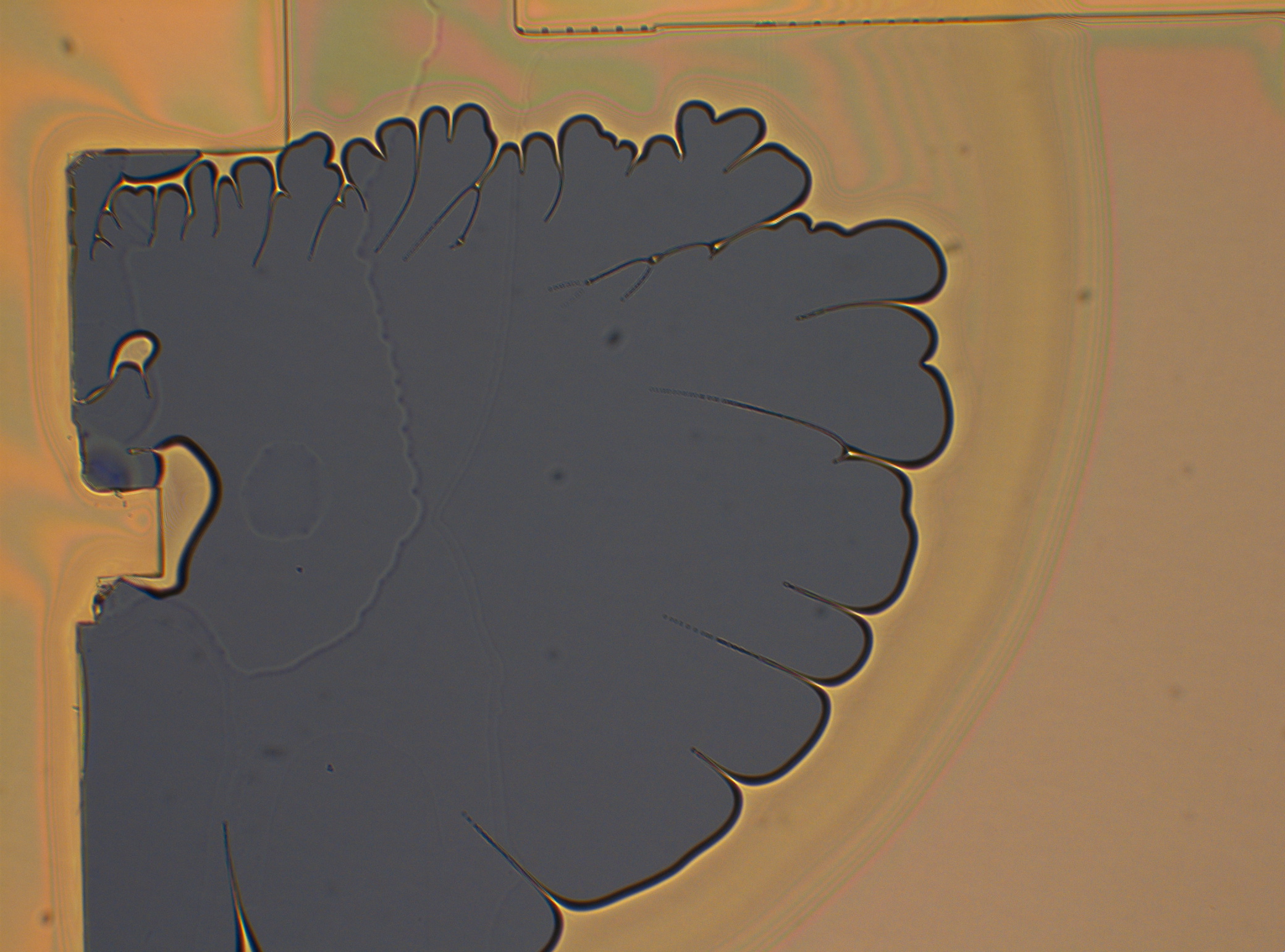
Post-Unaxis-Oxide-Deposition Failed Photoresist Spin - Media:J_badPRspin.jpg - Recipe Barton_SiO2_50C. Solution: solvent clean, dehydration bake, 2 min PEII at 200W
IVs spot Check 1_28_13 - File:IVs - Preliminary - 1 28 13.zip
LIVs 2_1_13 - File:LIVs - 2 1 13.zip
LIVs 2_4_13 - File:LIVs - 2 4 13.zip
LIVs in Excel - SGDBR 29 Lasers found - File:LIVs Excel.zip
Chip K - Vernier 05 - LIV and OSA data - File:K R1C2 Vernier05.xlsx
aSI PHASE MODULATOR RUN - Sweeper 3.1
Run 1
Step - Description - Sample Names - File
3.3 - Rib litho pics before hard mask etch: File:Rib litho pics.zip
3.4 - Rib Pics before Si Etch - Dummy 1 : File:Dummy post pr strip pre rib etch.zip
3.4 - Rib Pics before Si Etch - Sample 1: File:Sample1 pre si etch.zip
3.4 - Rib Pics before Si Etch - Sample 2: File:Sample2 pre si etch.zip
3.5 - Rib Pics post Si Etch - Sample 2: File:Sample2 post si etch.zip
Run 2
File:P1vid.zip
Step - Description - Sample Names - File
3.5 - SEM post Si Etch - Dummy 2: File:Dummy2 SEM post si etch.zip
4.4 - N-Dope Litho (Implant 3A) - Sample 3 & 4: File:Ndopelithopics.zip
4.5 - Post Implant 3A PR Strip - Sample 3 & 4: File:Post imp3A PR strip.zip
5.3 - P-Dope1 Litho (Implant 3B) - Sample 3 & 4: File:Implant3B litho.zip
5.4 - Post Implant 3B PR Strip: Media:post_imp3B_PR_strip.jpg
6.3 - P-Dope2 Litho (Implant 3C) - Sample 3 & 4: File:Implant3C litho.zip
6.4 - Post Implant 3C Partial PR Strip, "Cracks" - S3_Dies 1,2: File:Cracking Pics post 3C Strip 1.jpg
7.1 - Post 1050C Anneal (S3 and Dum2 taken to unknown temp): File:Post 1050C anneal pics.zip
9.2 - Via 1 Litho - Dum2, S3, S4: File:Via 1 litho pics.zip
9.4 - Via 1 Etched, PR Stripped: File:Via1 Etch PR Stripped.zip
10.1 - Failed Contact (NMetal) Litho - Dum2, S3, S4: File:Failed contact Litho.zip
10.1 - Contact (NMetal) Litho - File:NMetal Litho.zip
10.3 - Contact Metal Liftoff - File:Liftoff Results.zip
12.2 - Via 2 Litho - File:Via2Litho.zip
12.3 - Post 5 & 10 min SU8 etch - File:Post5and10minetchsu8.zip
12.. - SU8 Removal - SiNetch 2.5' + SU8 etch 3.5'+3.5' + ISO u/s 5' + Piranha 1' - File:Su8removalpostpiranhadip.zip
13.1 - SU8 Swabbed off/ PRMetal Litho - Sample 4 - File:SwabbingSU8 & ProbeMetalLitho.zip
13.4 - 2nd PRMetal Layer Lifted off - Sample 4 - File:2nd PRMetal Layer 9 5 12.zip
14.4 - Post Grating Opening Etch/Strip - Sample 4 - File:9 7postGOstrip.zip
PASSIVES RUN
Passive grating results: File:Sweeper Q2.doc
2D beam steering results, OFC video: File:OFC Doylend vid2.zip