File list
From OptoelectronicsWiki
This special page shows all uploaded files.
| Name | Thumbnail | Size | User | Description | Versions | |
|---|---|---|---|---|---|---|
| 09:12, 10 September 2012 | 9 7 DUV SOI 170 1 Sidewalls.zip (file) | 2.64 MB | Jaredhulme | Sidewall profiles of silicon wafer on best resolution and energy, ie Res = -.15 Energy = 25mJ/cm^2 | 1 | |
| 09:14, 6 September 2012 | SWEEPER 3 1 - aSi Shortloop v12B (EBL incl).zip (file) | 34.22 MB | JKD | 1 | ||
| 11:10, 5 September 2012 | Lab guidelines NOV2010.pdf (file) | 569 KB | Molly | 2 | ||
| 16:55, 4 September 2012 | 8 31 DUV SOI 170C 1.zip (file) | 1.47 MB | Jaredhulme | More SEMs of the SOI wafer Focus/Energy matrix. | 1 | |
| 12:39, 28 August 2012 | EAM11 implantation.zip (file) | 768 KB | Yongbo | 2 | ||
| 12:36, 28 August 2012 | EAM11 ARCoating.zip (file) | 60 KB | Yongbo | 1 | ||
| 12:30, 28 August 2012 | EAM11 mask overview.pptx (file) | 216 KB | Yongbo | 1 | ||
| 12:09, 28 August 2012 | EAM11 mask map.pptx (file) | 347 KB | Yongbo | 1 | ||
| 11:36, 28 August 2012 | DUV Stepper Waveguides v5.pptx (file) | 30.88 MB | Jaredhulme | 1 | ||
| 10:46, 28 August 2012 | 8 28 DUV SOI 170C 1.zip (file) | 1.89 MB | Jaredhulme | SOI wafer with matrix array. SEMs are named as E25_F-.15_HGRT, where 'E' stands for the energy in mJ/cm^2 and 'F' for the focus. Energy 25mJ/cm^2, Focus -.15 seems to be a good configuration. | 1 | |
| 10:42, 27 August 2012 | POEMv1Sim.zip (file) | 170 KB | Yongbo | 1 | ||
| 09:46, 27 August 2012 | SOI 500nm 1000nm spec.pdf (file) | 37 KB | Yongbo | 1 | ||
| 09:42, 27 August 2012 | POEMv1Code.zip (file) | 10 KB | Yongbo | 2 | ||
| 09:39, 27 August 2012 | POEMv1Final.zip (file) | 15.31 MB | Yongbo | 1 | ||
| 12:52, 23 August 2012 | Wavelength scan.zip (file) | 34 KB | Sudharsanan | 1 | ||
| 10:20, 23 August 2012 | 8 23 DUV SOI 170C 1.zip (file) | 1.34 MB | Jaredhulme | SOI wafer with matrix array. SEMs are named as E25_F-.15_HGRT, where 'E' stands for the energy in mJ/cm^2 and 'F' for the focus. It appears that the focus needs to be more negative than the current array. More SEMs are needed for conclusive proof. | 1 | |
| 12:56, 22 August 2012 | Post5and10minetchsu8.zip (file) | 1.96 MB | Jaredhulme | Looks ok but hard to tell if completely gone. I still need to do the last 30 SiN etch. Measurements over large window was 2.51 um with resist, 2.40 um post 5 min etch (resist gone), 2.38 um post another 5 min etch. | 1 | |
| 12:52, 22 August 2012 | Via2Litho.zip (file) | 495 KB | Jaredhulme | Notice the rounding at the top of the resist after the 10min 120C bake. | 1 | |
| 12:45, 22 August 2012 | NMetal Litho.zip (file) | 3.1 MB | Jaredhulme | Pictures of NMetal litho. Note the shifted alignment (at this and previous layers) on the serpentine waveguides vs the equal alignment on the straight waveguides. | 1 | |
| 12:39, 22 August 2012 | Liftoff Results.zip (file) | 3.26 MB | Jaredhulme | The test wafers with metal dep from yesterday ( 0.9 and 1.8 um resist) lifting off this morning with a pipet. Tey were soaked overnight in Acetone and no U/S. Still areas of large flaps but good enough to proceed with the dummy chip. The 0.9 um resist l | 1 | |
| 10:13, 17 August 2012 | DUV Stepper Waveguides v4.pptx (file) | 26.99 MB | Jaredhulme | 1 | ||
| 10:12, 17 August 2012 | DUV Stepper Waveguides v3.pptx (file) | 23.26 MB | Jaredhulme | 1 | ||
| 10:11, 17 August 2012 | DUV Stepper Waveguides v2.pptx (file) | 23.11 MB | Jaredhulme | 1 | ||
| 10:10, 17 August 2012 | DUV Stepper Waveguides v1.pptx (file) | 4.84 MB | Jaredhulme | 1 | ||
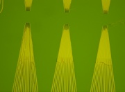
| 08:54, 17 August 2012 | DUV si 170C 2.jpg (file) |  |
225 KB | Jaredhulme | Microscope picture of the sample. Flood exposed before etch, developed after etch (AZ300MIF) | 1 |
| 08:50, 17 August 2012 | DUV-si-170C-1.zip (file) | 1.88 MB | Jaredhulme | SEMs of sample after WG etch and PR strip -PE2 2min, 1165 soak 30min, 1165 U/S (high, freq5, int5) 10 min, PE2 2min | 1 | |
| 21:09, 14 August 2012 | POEMv1ForReview.zip (file) | 2.69 MB | Yongbo | 2 | ||
| 12:51, 14 August 2012 | 160c 8 6 12.zip (file) | 3.8 MB | Jaredhulme | Silicon wafer - DBARC bake temperature 160C | 1 | |
| 12:50, 14 August 2012 | 180c 8 6 12.zip (file) | 4.61 MB | Jaredhulme | Silicon wafer - DBARC bake temperature 180C | 1 | |
| 12:48, 14 August 2012 | 180c 8 4 12.zip (file) | 2.9 MB | Jaredhulme | Silicon wafer - DBARC bake temperature 180C | 1 | |
| 12:48, 14 August 2012 | 170c 8 4 12.zip (file) | 2.18 MB | Jaredhulme | Silicon wafer - DBARC bake temperature 170C | 1 | |
| 11:00, 14 August 2012 | Post 1050C anneal pics.zip (file) | 2.93 MB | Jaredhulme | 2 | ||
| 09:51, 14 August 2012 | Failed contact Litho.zip (file) | 2.95 MB | Jaredhulme | Contact lithography, post SPR955CM-1.8 develop. Contact metal pad separation is 1um in some places and is getting undercut during the develop. This leads to strings of resist shifting position. | 1 | |
| 09:35, 14 August 2012 | Dummy2 SEM post si etch.zip (file) | 3.02 MB | Jaredhulme | SEMs of Dummy 2, post silicon rib etch | 1 | |
| 14:07, 13 August 2012 | POEMv1.pptx (file) | 157 KB | Yongbo | 1 | ||
| 13:43, 10 August 2012 | Post 20min NanoStrip 8 10 12.zip (file) | 542 KB | Jaredhulme | 1 | ||
| 09:32, 10 August 2012 | Via1 Etch PR Stripped.zip (file) | 200 KB | Jaredhulme | 1 | ||
| 09:32, 10 August 2012 | Via 1 litho pics.zip (file) | 2.67 MB | Jaredhulme | 1 | ||
| 09:22, 10 August 2012 | Via1 litho pics.zip (file) | 2.3 MB | Jaredhulme | 1 | ||
| 15:47, 9 August 2012 | KeyFinderInstaller.rar (file) | 1,017 KB | Jock | 1 | ||
| 00:56, 9 August 2012 | DUV Stepper Waveguides Development.pptx (file) | 23.26 MB | Jock | 3 | ||
| 17:27, 6 August 2012 | DUV Stepper Waveguides 2.pptx (file) | 23.11 MB | Jaredhulme | 1 | ||
| 16:35, 6 August 2012 | Cracking Pics post 3C Strip 1.jpg (file) | 3.05 MB | Jaredhulme | 1 | ||
| 16:28, 6 August 2012 | Cracking Pics post 3C Strip .jpg (file) | 3.06 MB | Jaredhulme | 1 | ||
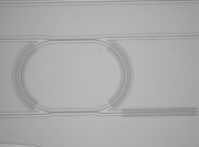
| 13:49, 6 August 2012 | Post imp3B PR strip.jpg (file) |  |
165 KB | Jaredhulme | 1 | |
| 13:35, 6 August 2012 | Implant3C litho.zip (file) | 994 KB | Jaredhulme | 1 | ||
| 08:43, 5 August 2012 | SWEEPER 3 1 - aSi Shortloop v12.zip (file) | 33.55 MB | JKD | zipped .cif file | 1 | |
| 08:41, 5 August 2012 | SWEEPER 3 1 - aSi Shortloop v12.cif (file) | 33.55 MB | JKD | 1 | ||
| 16:08, 2 August 2012 | Silicon Photonics The State of the Art - Graham Reed.rar (file) | 24.9 MB | Jock | 1 | ||
| 16:08, 2 August 2012 | Silicon Photonics An Introduction - Graham Reed.rar (file) | 1.63 MB | Jock | 1 |
 First page |
 Previous page |
 Next page |
 Last page |