File list
From OptoelectronicsWiki
This special page shows all uploaded files.
| Name | Thumbnail | Size | User | Description | Versions | |
|---|---|---|---|---|---|---|
| 15:59, 29 January 2013 | J badPRspin.jpg (file) |  |
856 KB | Jaredhulme | 1 | |
| 15:58, 29 January 2013 | QWetch.zip (file) | 3.96 MB | Jaredhulme | 1 | ||
| 15:56, 29 January 2013 | PMEtch.zip (file) | 1.93 MB | Jaredhulme | 1 | ||
| 15:54, 29 January 2013 | SW4 1 MesaEtch Rie2Traces.zip (file) | 115 KB | Jaredhulme | 1 | ||
| 15:49, 29 January 2013 | Via1Litho K R1C1.zip (file) | 193 KB | Jaredhulme | 1 | ||
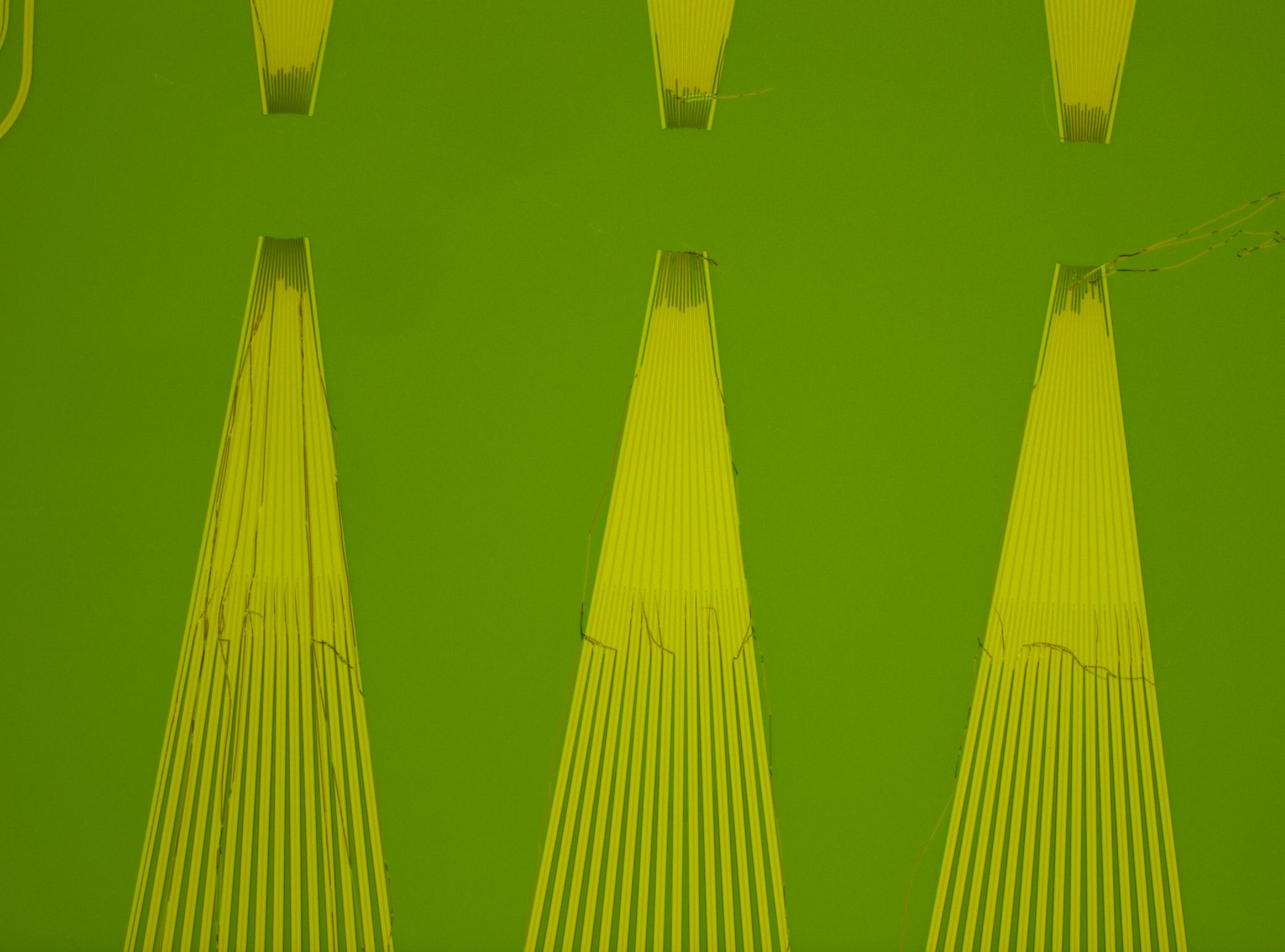
| 13:07, 29 January 2013 | NInP Etch K 1.png (file) |  |
5.98 MB | Jaredhulme | 1 | |
| 13:06, 29 January 2013 | Nmetalliftoff.zip (file) | 4.24 MB | Jaredhulme | 1 | ||
| 13:05, 29 January 2013 | Nmetallithochipi.zip (file) | 928 KB | Jaredhulme | 1 | ||
| 20:36, 30 November 2012 | SW4 1 PostBond+100nmOxide Microscopic.zip (file) | 6.28 MB | Jaredhulme | 1 | ||
| 20:35, 30 November 2012 | SW4 1 PostBond+100nmOxide Macroscopic.zip (file) | 5.25 MB | Jaredhulme | 1 | ||
| 17:19, 12 November 2012 | DUV Stepper Waveguides v8a.pptx (file) | 42.24 MB | Jaredhulme | With deep etch SEMs and AFM roughness | 1 | |
| 11:12, 12 November 2012 | DUV Stepper Waveguides v8.pptx (file) | 42.24 MB | Jaredhulme | Added Deep Etch photos for SOI wafer Energy 25, Focus -.15. | 1 | |
| 09:44, 12 November 2012 | 11 9 12 DUV SOI 1 DeepEtch.zip (file) | 2.85 MB | Jaredhulme | SEMs after deep etch for the center die (Energy 25, Focus-.15). | 1 | |
| 11:56, 24 October 2012 | ImportFiles.txt (file) | 4 KB | Jaredhulme | Uses macros to import a folder of text files into Excel. Files may have as many columns as desired and you can select which ones to import. To use, open Excel. Choose the View menu and click on Macros (at the far right). Choose a name for the mac... | 1 | |
| 11:51, 15 October 2012 | CurrentSweep.txt (file) | 4 KB | Jaredhulme | Added comments | 2 | |
| 16:27, 24 September 2012 | DUV Stepper Waveguides v7.pptx (file) | 37.91 MB | Jaredhulme | Added SEMs of Zig Zag Gratings designed by Mike Davenport (slide 53). | 1 | |
| 12:39, 11 September 2012 | 9 11duvzigzaggrating.zip (file) | 456 KB | Jaredhulme | 1 | ||
| 12:20, 10 September 2012 | Su8removalpostpiranhadip.zip (file) | 1.64 MB | Jaredhulme | 1 | ||
| 12:17, 10 September 2012 | SwabbingSU8 & ProbeMetalLitho.zip (file) | 1.97 MB | Jaredhulme | 1 | ||
| 12:07, 10 September 2012 | 9 7postGOstrip.zip (file) | 3.9 MB | Jaredhulme | 1 | ||
| 12:07, 10 September 2012 | 2nd PRMetal Layer 9 5 12.zip (file) | 3.41 MB | Jaredhulme | 1 | ||
| 09:35, 10 September 2012 | DUV Stepper Waveguides v6.pptx (file) | 37.24 MB | Jaredhulme | Added sidewall profiles (slides 48-52), additional pictures for SOI matrix (slides 67-69), and some conclusions (slides 54,77). | 2 | |
| 09:12, 10 September 2012 | 9 7 DUV SOI 170 1 Sidewalls.zip (file) | 2.64 MB | Jaredhulme | Sidewall profiles of silicon wafer on best resolution and energy, ie Res = -.15 Energy = 25mJ/cm^2 | 1 | |
| 16:55, 4 September 2012 | 8 31 DUV SOI 170C 1.zip (file) | 1.47 MB | Jaredhulme | More SEMs of the SOI wafer Focus/Energy matrix. | 1 | |
| 11:36, 28 August 2012 | DUV Stepper Waveguides v5.pptx (file) | 30.88 MB | Jaredhulme | 1 | ||
| 10:46, 28 August 2012 | 8 28 DUV SOI 170C 1.zip (file) | 1.89 MB | Jaredhulme | SOI wafer with matrix array. SEMs are named as E25_F-.15_HGRT, where 'E' stands for the energy in mJ/cm^2 and 'F' for the focus. Energy 25mJ/cm^2, Focus -.15 seems to be a good configuration. | 1 | |
| 10:20, 23 August 2012 | 8 23 DUV SOI 170C 1.zip (file) | 1.34 MB | Jaredhulme | SOI wafer with matrix array. SEMs are named as E25_F-.15_HGRT, where 'E' stands for the energy in mJ/cm^2 and 'F' for the focus. It appears that the focus needs to be more negative than the current array. More SEMs are needed for conclusive proof. | 1 | |
| 12:56, 22 August 2012 | Post5and10minetchsu8.zip (file) | 1.96 MB | Jaredhulme | Looks ok but hard to tell if completely gone. I still need to do the last 30 SiN etch. Measurements over large window was 2.51 um with resist, 2.40 um post 5 min etch (resist gone), 2.38 um post another 5 min etch. | 1 | |
| 12:52, 22 August 2012 | Via2Litho.zip (file) | 495 KB | Jaredhulme | Notice the rounding at the top of the resist after the 10min 120C bake. | 1 | |
| 12:45, 22 August 2012 | NMetal Litho.zip (file) | 3.1 MB | Jaredhulme | Pictures of NMetal litho. Note the shifted alignment (at this and previous layers) on the serpentine waveguides vs the equal alignment on the straight waveguides. | 1 | |
| 12:39, 22 August 2012 | Liftoff Results.zip (file) | 3.26 MB | Jaredhulme | The test wafers with metal dep from yesterday ( 0.9 and 1.8 um resist) lifting off this morning with a pipet. Tey were soaked overnight in Acetone and no U/S. Still areas of large flaps but good enough to proceed with the dummy chip. The 0.9 um resist l | 1 | |
| 10:13, 17 August 2012 | DUV Stepper Waveguides v4.pptx (file) | 26.99 MB | Jaredhulme | 1 | ||
| 10:12, 17 August 2012 | DUV Stepper Waveguides v3.pptx (file) | 23.26 MB | Jaredhulme | 1 | ||
| 10:11, 17 August 2012 | DUV Stepper Waveguides v2.pptx (file) | 23.11 MB | Jaredhulme | 1 | ||
| 10:10, 17 August 2012 | DUV Stepper Waveguides v1.pptx (file) | 4.84 MB | Jaredhulme | 1 | ||
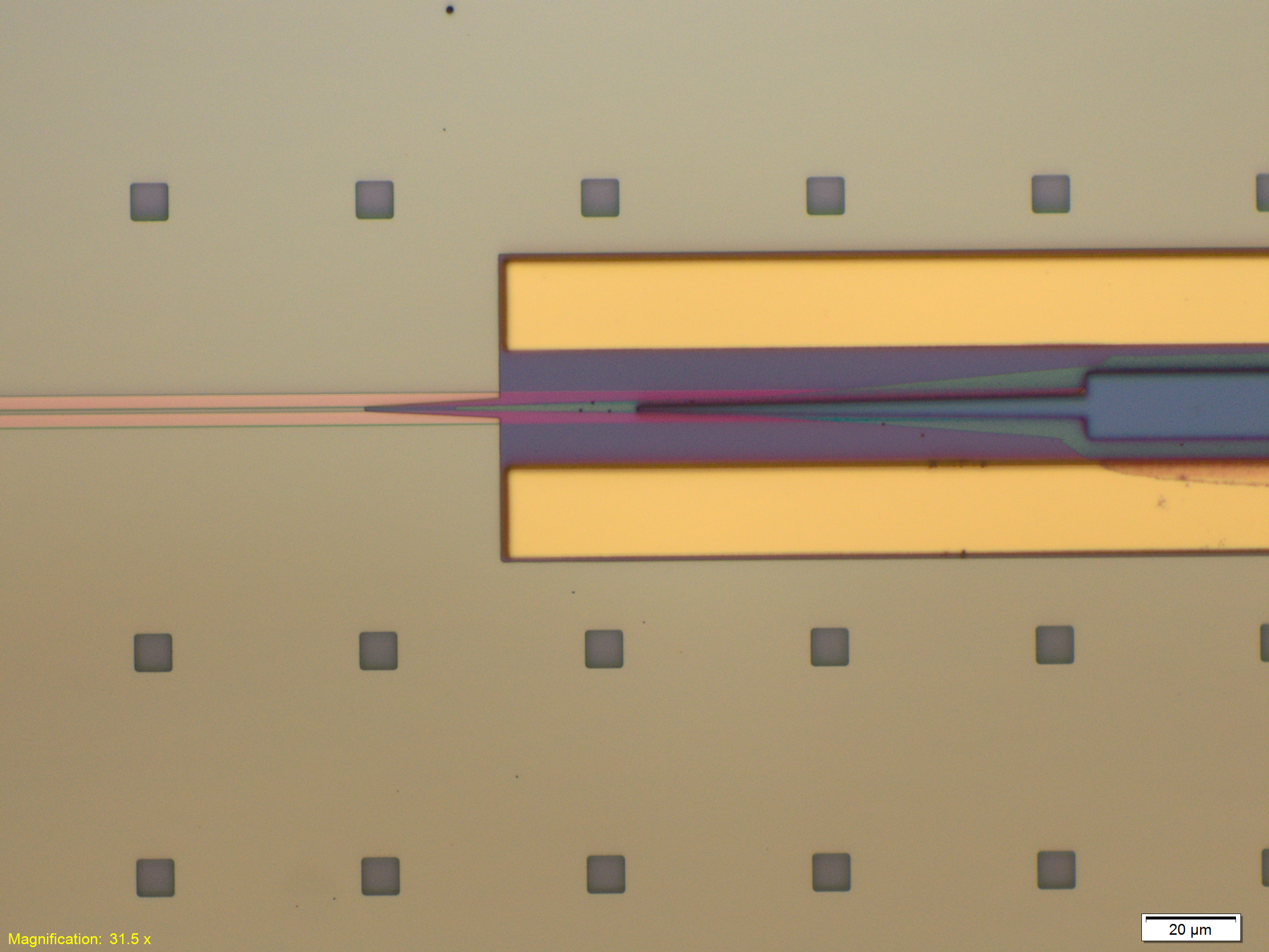
| 08:54, 17 August 2012 | DUV si 170C 2.jpg (file) |  |
225 KB | Jaredhulme | Microscope picture of the sample. Flood exposed before etch, developed after etch (AZ300MIF) | 1 |
| 08:50, 17 August 2012 | DUV-si-170C-1.zip (file) | 1.88 MB | Jaredhulme | SEMs of sample after WG etch and PR strip -PE2 2min, 1165 soak 30min, 1165 U/S (high, freq5, int5) 10 min, PE2 2min | 1 | |
| 12:51, 14 August 2012 | 160c 8 6 12.zip (file) | 3.8 MB | Jaredhulme | Silicon wafer - DBARC bake temperature 160C | 1 | |
| 12:50, 14 August 2012 | 180c 8 6 12.zip (file) | 4.61 MB | Jaredhulme | Silicon wafer - DBARC bake temperature 180C | 1 | |
| 12:48, 14 August 2012 | 180c 8 4 12.zip (file) | 2.9 MB | Jaredhulme | Silicon wafer - DBARC bake temperature 180C | 1 | |
| 12:48, 14 August 2012 | 170c 8 4 12.zip (file) | 2.18 MB | Jaredhulme | Silicon wafer - DBARC bake temperature 170C | 1 | |
| 11:00, 14 August 2012 | Post 1050C anneal pics.zip (file) | 2.93 MB | Jaredhulme | 2 | ||
| 09:51, 14 August 2012 | Failed contact Litho.zip (file) | 2.95 MB | Jaredhulme | Contact lithography, post SPR955CM-1.8 develop. Contact metal pad separation is 1um in some places and is getting undercut during the develop. This leads to strings of resist shifting position. | 1 | |
| 09:35, 14 August 2012 | Dummy2 SEM post si etch.zip (file) | 3.02 MB | Jaredhulme | SEMs of Dummy 2, post silicon rib etch | 1 | |
| 13:43, 10 August 2012 | Post 20min NanoStrip 8 10 12.zip (file) | 542 KB | Jaredhulme | 1 | ||
| 09:32, 10 August 2012 | Via1 Etch PR Stripped.zip (file) | 200 KB | Jaredhulme | 1 | ||
| 09:32, 10 August 2012 | Via 1 litho pics.zip (file) | 2.67 MB | Jaredhulme | 1 | ||
| 09:22, 10 August 2012 | Via1 litho pics.zip (file) | 2.3 MB | Jaredhulme | 1 | ||
| 17:27, 6 August 2012 | DUV Stepper Waveguides 2.pptx (file) | 23.11 MB | Jaredhulme | 1 | ||
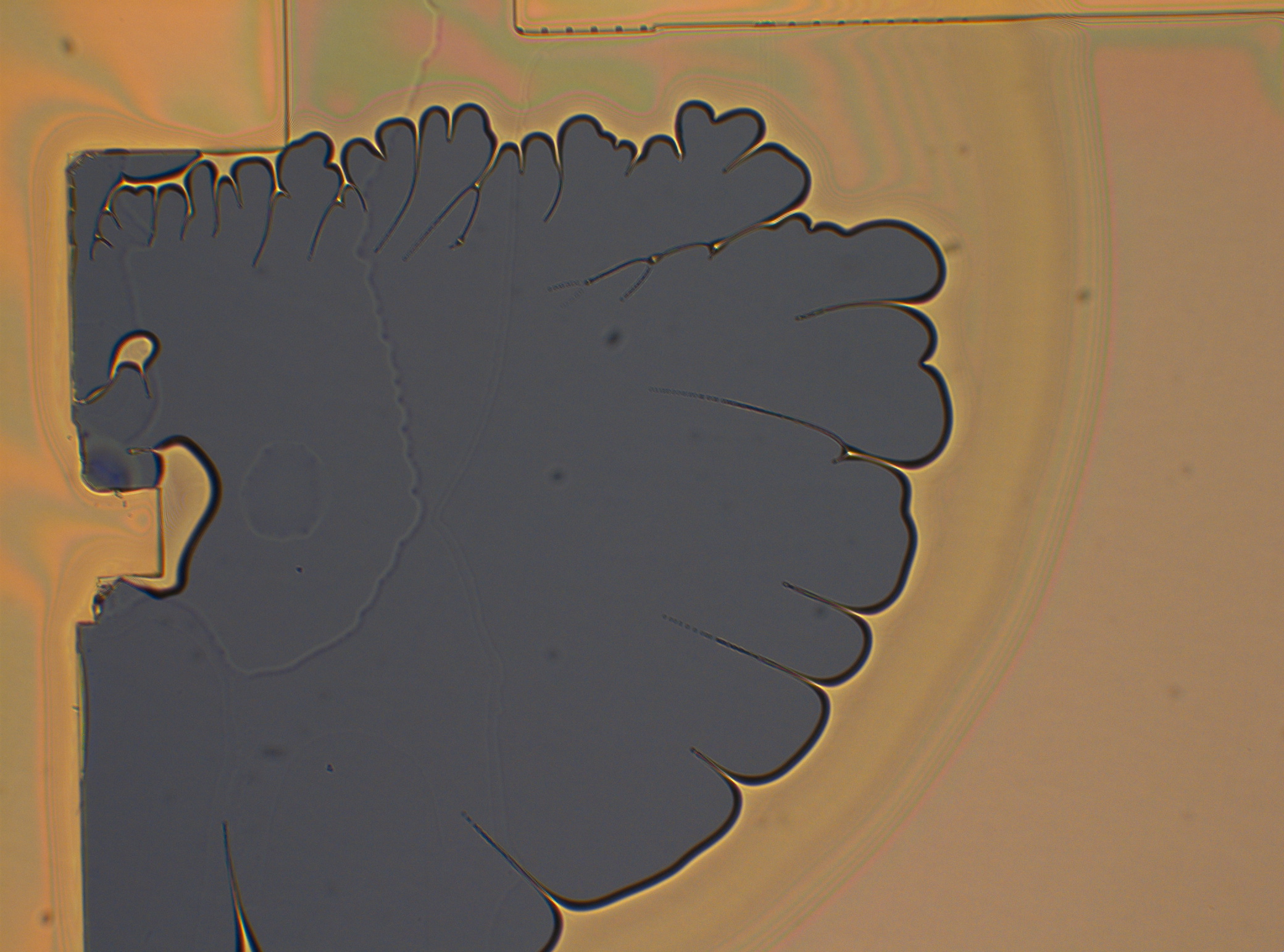
| 16:35, 6 August 2012 | Cracking Pics post 3C Strip 1.jpg (file) |  |
3.05 MB | Jaredhulme | 1 |
First page |
Previous page |
Next page |
Last page |